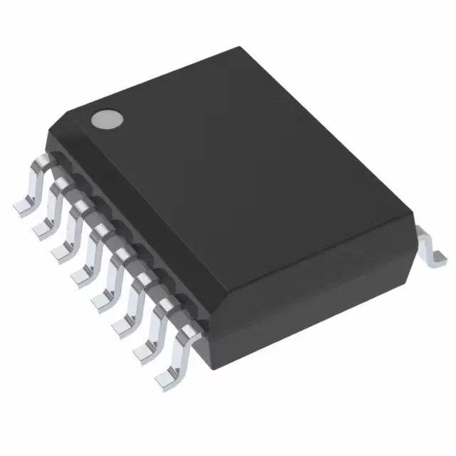
It uses a Quad I/O SPI interface running at 66 MHz, which gives you four times the read throughput of a standard SPI bus — useful for XiP (execute-in-place) or fast firmware staging without a separate RAM buffer. The supply range is 2.7V to 3.6V, so it sits comfortably on a 3.3V rail with margin for brownout.
66 MHz clock and Quad I/O — throughput for code shadowing
At 66 MHz in Quad I/O mode, the S25FL512SDPMFIG10 can sustain read throughput around 264 Mbps (66 MHz × 4 lanes). That is fast enough to shadow a 512 Mbit firmware image into RAM in under two seconds, or to run code directly from the flash with minimal wait states on a moderate-speed MCU. The 66 MHz figure is the maximum clock — derate for longer PCB traces or higher capacitive loads, but for a typical 16-SOIC layout on a 4-layer board it holds without issues.
That means it is suitable for outdoor telecom cabinets, factory automation controllers, and HVAC systems — anything that sees seasonal temperature swings but stays above the freezing point of water. If your design needs -40°C to 105°C or 125°C (automotive under-hood), you would need a different temperature grade variant in the FL-S family.
The base product number is S25FL512, so future density or package variants in the same family share the same command set and footprint.