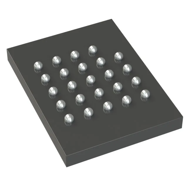
Package and board-fit — 24-ball BGA, 8×6 mm
The S25FL512SDPBHBC13 ships in a 24-ball TBGA (thin fine-pitch BGA) with a 8×6 mm body — the 0.80 mm ball pitch demands a four-layer PCB for fan-out; two-layer boards will struggle to route the inner balls without buried vias. The package is RoHS-compliant and supplied on tape and reel (TR) for automated pick-and-place. No exposed thermal pad — the die heat dissipates through the BGA balls and the board copper plane.
Clock speed and bus margin — 66 MHz Quad I/O
The SPI interface runs up to 66 MHz in Quad I/O mode — that is 264 Mbit/s effective throughput on a four-lane bus, enough to feed a Cortex-M7 instruction cache without wait-state stalls on sequential reads. The actual sustained read rate depends on the controller's SPI FIFO depth and the flash's initial access latency (the first read command incurs a dummy-cycle overhead before data appears on the bus).
Temperature grade and deployment — industrial range
The 105°C ceiling gives margin above the typical 85°C industrial limit, so the part stays within the absolute-maximum junction temperature even under self-heating during sustained reads.