512 Mbit NOR Flash with Quad-SPI — what the 133 MHz clock buys you
The Infineon S25FL512SAGBHVC13 is a 512 Mbit (organized as 64M x 8) NOR Flash memory from the FL-S series, built for code-shadowing and data-logging in industrial and communications equipment.
BGA footprint and layout — what the 24-ball package changes
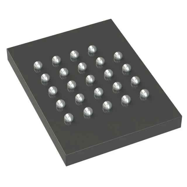
This part comes in a 24-ball TBGA (8 mm x 6 mm body), supplier package code 24-BGA. The ball pitch is 0.8 mm typical for this class — tight enough that a two-layer PCB with via-in-pad can work, but the decoupling cap placement needs to sit within 3 mm of the supply balls to keep the 133 MHz edge clean. If your rework station handles 0.8 mm pitch BGA, this is a straightforward reball.
If you are qualifying a second source for supply resilience, the FL-S family includes multiple density and package variants that share the same SPI command set — the firmware driver port is usually a matter of adjusting the sector erase granularity, not rewriting the low-level layer.
What the specs mean for firmware and system design
The 133 MHz clock frequency is the ceiling for the SPI bus — the actual throughput depends on the host controller's ability to sustain back-to-back quad reads without wait states. The 512 Mbit (64 MB) capacity is sized for a combined bootloader + application image + file system.