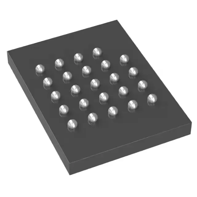
The Cypress S25FL512SAGBHI210 is a 512 Mbit FL-S series NOR Flash memory configured as 64M x 8 bits, accessed through a SPI Quad I/O interface at up to 133 MHz. The Quad-SPI protocol gives you four data lines for read operations, effectively quadrupling the throughput over standard SPI without adding extra controller pins. This part is organized for non-volatile storage of firmware images, configuration tables, and boot code in embedded systems where the SPI controller is already on the MCU or SoC.
Supply voltage and temperature — industrial reliability
At 85°C junction, the SPI bus timing still holds the 133 MHz spec — the FL-S family was designed with enough timing margin that a 30% eye opening at 104 MHz is documented in application notes.
Housed in a 24-ball TBGA measuring 8x6 mm (supplier device package 24-BGA). Surface-mount only, and the BGA footprint means the board house needs x-ray inspection after reflow to check for solder voids under the balls. If you are doing rework in a lab, the standard hot-air profile for a 0.8 mm pitch BGA works, but pre-bake at 125°C for 8 hours if the moisture-barrier bag has been open past the floor-life window — MSL 3 is the default for this package class. The tray shipping medium tells you these come in antistatic trays, not tape-and-reel, so factor that into your pick-and-place feeder setup.
Listed as Active, meaning Cypress (now Infineon) continues to manufacture this part with no announced end-of-life. No last-time-buy calculus needed, no scramble for surplus lots. The base product number S25FL512 covers the whole density family, so if you ever need to scale up or down within the FL-S series, the pin-compatible siblings share the same footprint.