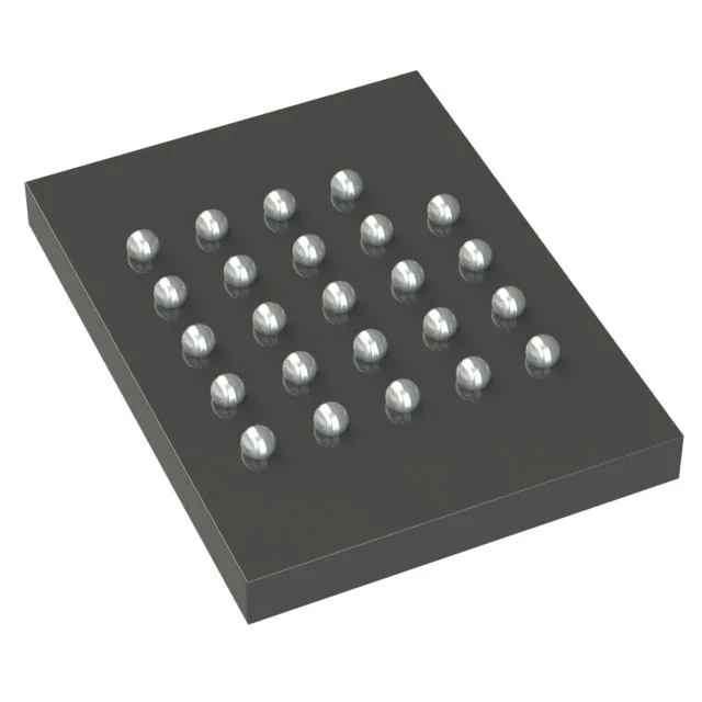
Automotive-grade NOR Flash for code shadowing and data logging
It uses a Quad SPI interface running at 133 MHz, which gives you fast read throughput for firmware shadowing or XIP (eXecute In Place) in an automotive ECU, ADAS module, or telematics unit.
The 133 MHz clock on the Quad-SPI interface translates to a theoretical read throughput of 532 Mbps (four data lines at 133 MHz). In practice, with command overhead and dummy cycles, you can expect around 50-70 MB/s sustained reads — enough to feed a high-end Cortex-R or Cortex-M core without stalling. The 64M x 8 organization (512 Mbit) means the memory array is byte-addressable, which simplifies firmware partitioning: one large code region or multiple smaller data logs.
AEC-Q100 qualification is not just a sticker — it means the part has passed a suite of reliability tests: high-temperature operating life (HTOL), temperature cycling, moisture sensitivity, and electrostatic discharge (HBM/CDM). For a production BOM in an automotive ECU, this qualification is often a gate requirement. The FL-S series is Infineon's mainstream automotive NOR Flash line, so you get a known track record and PCN/EOL support. The active lifecycle status means no near-term obsolescence risk — you can design it in without worrying about a last-time-buy window.
24-ball BGA footprint — layout notes
That is a standard, easy-to-route BGA — no micro-vias needed for most designs. The supplier device package is 24-BGA (8x6), so the footprint is consistent across the FL-S family. For decoupling, a 100 nF ceramic cap per supply pin pair, placed as close to the balls as the via pattern allows, keeps the supply clean at 133 MHz.