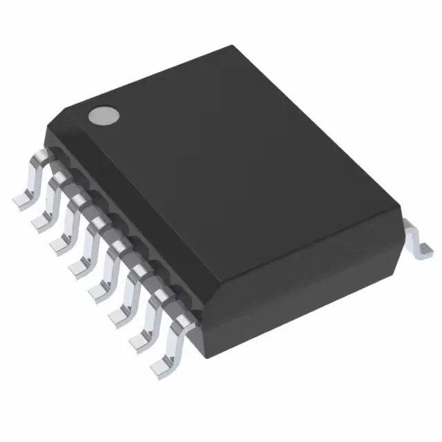
Infineon Technologies S25FL256SDSMFV010 — Memory (DRAM / SRAM / Flash / EEPROM)

S25FL256SDSMFV010 256 Mbit NOR Flash – Quad SPI, 80 MHz

MPNS25FL256SDSMFV010
Active

Infineon FL-S series, 256 Mbit NOR Flash, SPI Quad I/O interface, 80 MHz clock, 2.7V–3.6V supply, -40°C to 105°C, 16-SOIC (7.50mm width)

$6.5900Ref. price · indicative, final on quote
Sourced new & surplus through independent channelsAuthenticity-screened · ESD-safe packingListing updated Aug 2026

Specifications

S25FL256SDSMFV010 specifications
ParameterValue
SeriesFL-S
Memory typeNon-Volatile
MountingSurface Mount
Voltage2.7V ~ 3.6V
Frequency80 MHz
Memory interfaceSPI - Quad I/O
Operating temperature-40°C~105°C(TA)
PackageTray
TechnologyFLASH - NOR
Memory size256Mbit
Memory formatFLASH
Case16-SOIC (0.295\", 7.50mm Width)
Memory organization32M x 8

Product details

256 Mbit NOR Flash with Quad SPI for code and data storage

The S25FL256SDSMFV010 is a 256 Mbit (32M x 8) NOR Flash memory from Infineon's FL-S series, organized as 32M x 8 bits and accessed through an SPI Quad I/O interface running at up to 80 MHz. The Quad I/O mode reads four bits per clock cycle, delivering a sustained throughput of 40 MB/s without widening the package footprint beyond the standard 6-pin SPI bus — useful for execute-in-place (XIP) boot and high-speed firmware shadowing in systems where pin count is tight.

Operates from 2.7V to 3.6V, which aligns with common 3.3V logic rails used across MCU and SoC platforms.

Infineon lists the S25FL256SDSMFV010 as Active. Sourced per RFQ against your line-item quantity.

16-SOIC package — board-fit and rework considerations

Housed in a 16-SOIC (0.295-inch body width, 7.50 mm) surface-mount package with a 1.27 mm pitch — a common footprint that reflows on standard lead-free profiles and is inspectable without X-ray. The wide body width provides good thermal coupling to the PCB copper pour for heat spreading during erase/write cycles.

Frequently asked questions

Does S25FL256SDSMFV010 support Quad SPI?

Yes — the memory interface is SPI Quad I/O, which reads four data bits per clock cycle through the standard SPI pins. This quadruples the read throughput compared to single-bit SPI without adding package pins.

What is the erase block size for S25FL256SDSMFV010?

The evidence does not specify the erase block size. The datasheet should be consulted for sector and block architecture details.