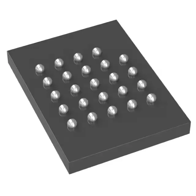
Infineon Technologies S25FL256SDSBHV213 — Memory (DRAM / SRAM / Flash / EEPROM)

S25FL256SDSBHV213 256 Mbit NOR Flash, 80 MHz Quad-SPI

MPNS25FL256SDSBHV213
Active

Infineon FL-S series S25FL256SDSBHV213, 256 Mbit NOR Flash, SPI Quad I/O interface, 80 MHz clock frequency, 2.7 V to 3.6 V supply, -40°C to 105°C, 24-TBGA package.

$5.0050Ref. price · indicative, final on quote
Sourced new & surplus through independent channelsAuthenticity-screened · ESD-safe packingListing updated Aug 2026

Specifications

S25FL256SDSBHV213 specifications
ParameterValue
SeriesFL-S
Memory typeNon-Volatile
MountingSurface Mount
Voltage2.7V ~ 3.6V
Frequency80 MHz
Memory interfaceSPI - Quad I/O
Operating temperature-40°C~105°C(TA)
PackageTape & Reel (TR)
TechnologyFLASH - NOR
Memory size256Mbit
Memory formatFLASH
Case24-TBGA
Memory organization32M x 8

Product details

256 Mbit NOR Flash for code shadow and OTA staging

The Infineon S25FL256SDSBHV213 is a 256 Mbit FL-S series NOR Flash memory organized as 32 M x 8 bits, accessed through a SPI Quad I/O interface clocked at 80 MHz. This part is the go-to for designs that need a reliable, high-density boot and code-storage NOR device with fast read throughput for execute-in-place (XIP) or shadow-to-RAM boot flows. The 80 MHz clock rate with Quad I/O yields a sustained read bandwidth that can keep a high-end MCU or FPGA configuration engine fed without wait states, assuming the host controller supports the Quad-SPI protocol. For firmware-over-the-air (OTA) applications, the 256 Mbit density provides ample staging space for a full-image backup plus active image, with room for configuration tables and calibration data.

Industrial temp range and BGA footprint

The 24-ball TBGA package (8 x 6 mm body) is a compact footprint for space-constrained designs, but demands careful PCB layout for signal integrity on the Quad-SPI lines and proper thermal management — the BGA's solder balls carry both electrical and thermal paths. Surface-mount assembly with the 24-BGA package requires standard reflow profiling for an MSL-rated device. The small ball pitch means the PCB pad design and solder paste volume need to match the package's coplanarity spec to avoid head-in-pillow defects. X-ray inspection post-reflow is recommended to verify ball wetting, especially on prototypes or first production runs.

For production planning, this removes the risk of forced redesigns or premium spot buys in the near term. The FL-S series is a mature, well-established NOR Flash family with broad ecosystem support, so firmware and hardware reference designs are stable.

Frequently asked questions

What is the clock frequency of S25FL256SDSBHV213?

The SPI Quad I/O interface supports a clock frequency of 80 MHz. At this rate, the Quad I/O mode delivers a theoretical read throughput of 320 Mbps (80 MHz x 4 data lines), sufficient for fast boot and XIP applications.

How does the S25FL256SDSBHV213 compare to other 256 Mbit NOR Flash parts?

Within the FL-S series, this part sits at the 256 Mbit density tier with Quad I/O and an 80 MHz clock. A sibling like the S25FL256SAGBHV200 also offers 256 Mbit but in a different package or with a slightly different feature set. The key decision factor is the 24-BGA footprint versus alternate package options — the pinout and electrical specs remain consistent across the FL-S family at the same density.

Where can I find the datasheet for S25FL256SDSBHV213?

The datasheet is available from Infineon's official website under the FL-S series documentation. It covers the full electrical characteristics, timing diagrams, command set, and package dimensions for the 24-BGA variant. Request a quote through this listing and we can include a datasheet link with your confirmation.