256 Mbit NOR Flash on Quad SPI — what this part is for
The 66 MHz clock frequency supports firmware shadowing and execute-in-place (XIP) boot in embedded systems where the MCU or FPGA boots directly from serial Flash. Typical applications include industrial controllers, networking equipment, and automotive telematics where non-volatile code storage and OTA update staging are needed.
66 MHz clock and Quad I/O — bus timing and throughput
The 66 MHz clock is the ceiling for this density variant in the FL-S family. At Quad I/O mode, four bits per clock cycle give an effective read throughput of about 33 MB/s, which is enough to feed a Cortex-M7 or a mid-range FPGA configuration controller without stalling. The interface is backward-compatible with single SPI, so a legacy bootloader that only drives MOSI/MISO can still read the device at reduced speed. The 2.7V to 3.6V supply range matches common 3.3V logic rails, but the lower end at 2.7V means the part stays alive through a brown-out that would drop a 3.0V-only Flash off the bus.
Industrial temperature grade — where it runs
The 105°C ceiling is the industrial-plus tier, not the full automotive 125°C grade, so for engine-mounted ECUs that see junction temperatures above 105°C you would step to the AEC-Q100 qualified FL-S variants. For chassis and cabin domains, this temperature range is comfortable.
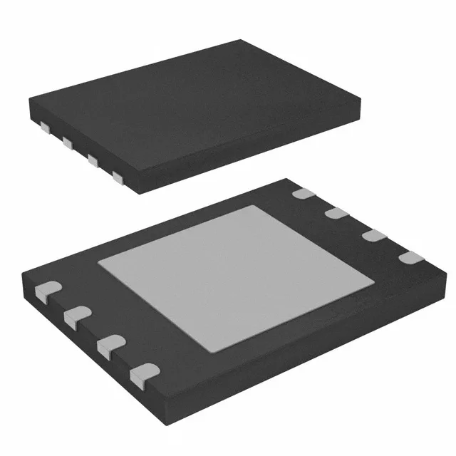
Package and footprint — 8-WSON with exposed pad
Without those vias, the junction temperature rises faster during continuous read bursts at 66 MHz. The Tape & Reel shipping format is standard for pick-and-place assembly.
The FL-S series has broad second-source coverage from Macronix and Winbond in the same 256 Mbit density and Quad I/O interface, but those are not pin-compatible — the footprint differs. For a drop-in replacement within the same family, the S25FL256SAGMFI003 is the standard-voltage sibling in a different package variant.