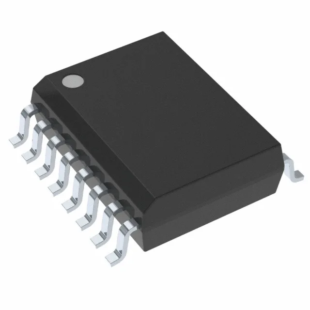
Infineon Technologies S25FL256SAGMFIR01 — Memory (DRAM / SRAM / Flash / EEPROM)

S25FL256SAGMFIR01 Infineon FL-S NOR Flash, 256 Mbit, 133 MHz

MPNS25FL256SAGMFIR01
Active

Infineon FL-S series, S25FL256SAGMFIR01, 256 Mbit NOR Flash, SPI Quad I/O interface, 133 MHz clock, 2.7-3.6 V supply, -40°C to 85°C, 16-SOIC (7.50 mm width), Tube.

$5.8400Ref. price · indicative, final on quote
Packaging16-SOIC (0.295", 7.50mm Width)
RoHSROHS3 Compliant
SeriesFL-S
Independent supplier — new & surplus stockAuthenticity-screened · ESD-safe packingListing updated Aug 2026

Specifications

S25FL256SAGMFIR01 specifications
ParameterValue
SeriesFL-S
Memory typeNon-Volatile
MountingSurface Mount
Voltage2.7V ~ 3.6V
Frequency133 MHz
Memory interfaceSPI - Quad I/O
Operating temperature-40°C ~ 85°C (TA)
PackageTube
TechnologyFLASH - NOR
Memory size256Mbit
Memory formatFLASH
Case16-SOIC (0.295\", 7.50mm Width)
Memory organization32M x 8

Product details

256 Mbit NOR Flash with Quad I/O at 133 MHz

The Infineon S25FL256SAGMFIR01 is a 256 Mbit FL-S series NOR Flash memory organized as 32 M x 8 bits, accessed through a SPI Quad I/O interface clocked at 133 MHz. It operates from a 2.7 V to 3.6 V supply and is rated for the -40°C to 85°C industrial temperature range. This part is designed for code-shadowing, execute-in-place (XIP), and firmware storage in embedded systems where fast read throughput and non-volatile retention are required.

133 MHz clock — read throughput for XIP

The 133 MHz SPI clock rate, combined with Quad I/O, delivers a sustained read throughput that supports execute-in-place without the latency of a DRAM shadow copy. The interface is backward-compatible with standard SPI and Dual I/O modes, so it drops into existing SPI bus topologies with a firmware change to enable the quad commands.

The -40°C to 85°C operating range and 2.7 V to 3.6 V supply rail are specified in the datasheet. The 16-SOIC package uses a standard JEDEC footprint.

Frequently asked questions

What is the maximum operating frequency of S25FL256SAGMFIR01?

The maximum clock frequency is 133 MHz for the SPI Quad I/O interface. This sets the peak read throughput for code-shadowing and XIP applications.

What is the footprint and pinout of S25FL256SAGMFIR01?

The package is a 16-SOIC with 0.295 inch body width (7.50 mm) — a standard JEDEC SOIC-16W footprint. The pinout follows the industry-standard SPI NOR Flash pin assignment for 16-pin SOIC. Verify against the Infineon datasheet land pattern before PCB layout.

Where can I buy S25FL256SAGMFIR01?

This part is available to order through independent distribution. Submit an RFQ for current pricing, stock position, and lead time — availability is confirmed at quote time.

What is the difference between S25FL256S and S25FL128S?

The S25FL256S offers 256 Mbit density; the S25FL128S is the 128 Mbit variant. Both share the FL-S series, Quad I/O interface, and 133 MHz clock. The density choice depends on your firmware image size and OTA update buffer requirements.