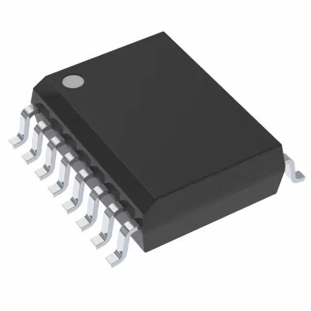
Its SPI Quad I/O interface pushes the clock to 133 MHz, delivering a sustained read rate that keeps a Cortex-M or RISC-V core fed during XIP (eXecute-In-Place) without waiting for a DRAM load. The 256 Mbit density (organized as 32M x 8) is a sweet spot for a single firmware image plus an OTA staging area in industrial controllers, networking gear, and automotive telematics units.
At 133 MHz the SPI clock period is about 7.5 ns. With Quad I/O, four data bits per clock cycle yield an effective throughput of 532 Mbps. That margin matters when the host controller runs at 200 MHz+ and the flash read latency must not stall the instruction prefetch. The part's internal latency and output hold times are spec'd for this clock rate; a slower part at 104 MHz would leave 22% less bandwidth on the table, which shows up as longer boot times or dropped frames in a data-logging pipeline.
Package and temperature — fit for the board and the environment
The 2.7V to 3.6V supply range covers the full 3.3V rail tolerance band, including the low end during a brown-out or cold-crank event.
No NRND or last-time-buy notice has been issued for this density-speed-package variant.