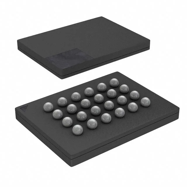
Infineon Technologies S25FL256SAGBHVD00 — Memory (DRAM / SRAM / Flash / EEPROM)

Infineon S25FL256SAGBHVD00 256Mbit NOR Flash, SPI Quad I/O

MPNS25FL256SAGBHVD00
Active

Infineon FL-S series NOR Flash memory, 256Mbit, SPI Quad I/O interface, 133 MHz clock, 2.7-3.6V supply, -40 to +105°C, 24-BGA (6x8mm) tray package, order code S25FL256SAGBHVD00.

$5.7900Ref. price · indicative, final on quote
Packaging24-TBGA
RoHSROHS3 Compliant
SeriesFL-S
Independent supplier — new & surplus stockAuthenticity-screened · ESD-safe packingListing updated Aug 2026

Specifications

S25FL256SAGBHVD00 specifications
ParameterValue
SeriesFL-S
Memory typeNon-Volatile
MountingSurface Mount
Voltage2.7V ~ 3.6V
Frequency133 MHz
Memory interfaceSPI - Quad I/O
Operating temperature-40°C ~ 105°C (TA)
PackageTray
TechnologyFLASH - NOR
Memory size256Mbit
Memory formatFLASH
Case24-TBGA
Memory organization32M x 8

Product details

Industrial temperature and Quad I/O throughput

The S25FL256SAGBHVD00: The SPI Quad I/O interface uses four data lines for reads and writes, cutting the number of bus cycles compared to standard SPI. This matters when the host MCU boots directly from flash or streams large look-up tables. The 2.7 V minimum supply means the part stays operational through a 3.3 V rail that droops under load — no brown-out reset until the rail drops below that floor.

BGA footprint and board-level integration

The 24-BGA package (6x8 mm) has a 0.80 mm ball pitch. The inner two rows of balls require via-in-pad or microvias on a standard 4-layer board — the outer rows fan out easily on the top layer. The supplier device package code is 24-BGA (6x8), so the land pattern is consistent across the FL-S family. No exposed thermal pad — the BGA relies on the PCB copper planes for heat spreading.

Frequently asked questions

What is the maximum clock frequency supported by S25FL256SAGBHVD00?

The maximum clock frequency is 133 MHz on the SPI Quad I/O interface.

Does S25FL256SAGBHVD00 have a standard JEDEC footprint layout?

The 24-ball BGA package (6x8 mm) follows the standard JEDEC MO-275 footprint for 0.80 mm pitch BGA devices. The land pattern is consistent across the FL-S family.

What is the difference between S25FL256SAGBHVD00 and S25FL256SAGBHI300?

Both are 256 Mbit FL-S NOR flash with the same 133 MHz Quad I/O interface and 24-BGA package. The BHVD00 is the wider-temperature variant.