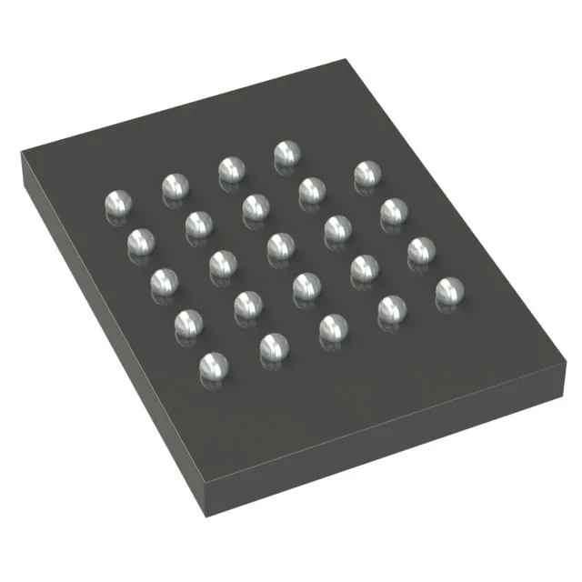
Infineon Technologies S25FL256SAGBHVC03 — Memory (DRAM / SRAM / Flash / EEPROM)

Infineon S25FL256SAGBHVC03 256 Mbit NOR Flash, 133 MHz

MPNS25FL256SAGBHVC03
Active

Infineon Technologies FL-S series NOR flash, S25FL256SAGBHVC03, 256 Mbit, SPI Quad I/O, 133 MHz, 2.7-3.6 V, -40 to 105°C, 24-BGA (8x6 mm), Tape & Reel.

$3.9978Ref. price · indicative, final on quote
Sourced new & surplus through independent channelsAuthenticity-screened · ESD-safe packingListing updated Aug 2026

Specifications

S25FL256SAGBHVC03 specifications
ParameterValue
SeriesFL-S
Memory typeNon-Volatile
MountingSurface Mount
Voltage2.7V ~ 3.6V
Frequency133 MHz
Memory interfaceSPI - Quad I/O
Operating temperature-40°C ~ 105°C (TA)
PackageTape & Reel (TR)
TechnologyFLASH - NOR
Memory size256Mbit
Memory formatFLASH
Case24-TBGA
Memory organization32M x 8

Product details

256 Mbit NOR flash with a 133 MHz Quad I/O bus

The S25FL256SAGBHVC03 is a 256 Mbit SPI NOR flash from Infineon's FL-S series, organized as 32M x 8 bits. The 133 MHz clock rate on the Quad I/O interface pushes the sustained read throughput well past what a single-bit SPI bus can deliver — useful when the MCU fetches code or logs data in bursts.

Supply rails and temperature grade

The -40°C to 105°C operating range covers the industrial temperature band — suitable for outdoor telecom cabinets, motor drives, and engine-bay electronics where the ambient climbs above 85°C.

24-ball BGA footprint and rework considerations

Packaged in a 24-ball TBGA (8x6 mm body). The 0.80 mm ball pitch is forgiving enough for a standard reflow profile without micro-vias, but the BGA package means the board-side pad finish and stencil aperture matter for solder-joint reliability. Pre-bake at 125°C for 8 hours if the parts have been exposed to ambient humidity beyond the MSL floor life — the BGA's plastic overmold can trap moisture.

Active lifecycle — no design-in clock ticking

Infineon lists this as an active part. The FL-S series has been a stable NOR flash line for years; the 256 Mbit density at 133 MHz is a common sweet spot for code-shadowing and data-logging applications.

Frequently asked questions

What interface does the S25FL256SAGBHVC03 use?

It uses an SPI Quad I/O interface. The 133 MHz clock rate with four I/O lanes gives a theoretical read throughput of 532 Mbps, though actual throughput depends on the controller's command overhead and the number of wait states.

What package does the S25FL256SAGBHVC03 come in?

A 24-ball TBGA (8x6 mm body). The 0.80 mm ball pitch is standard for this density and allows routing on a 4-layer board without blind vias.