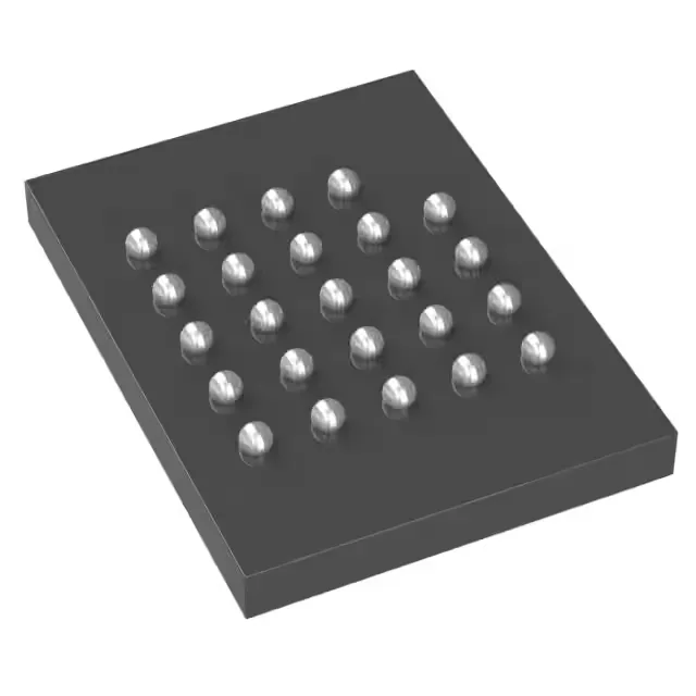
The Cypress S25FL256SAGBHIA13 is a 256 Mbit serial NOR Flash memory from the FL-S family, organized as 32M x 8 bits. The 133 MHz clock frequency gives a theoretical Quad read throughput of 532 Mbps, which is the figure that matters when sizing the code shadowing time or the data-logging bandwidth in an embedded system. It comes in a 24-ball TBGA package measuring 8 mm x 6 mm — a compact footprint that saves board area but requires BGA assembly and X-ray inspection.
The FL-S series is a mature, widely used NOR Flash family, so supply is stable through both authorized and independent channels.
Quad I/O at 133 MHz — why the interface speed matters
The SPI Quad I/O interface is the main performance differentiator. Standard SPI uses one data line; Quad I/O uses four, quadrupling the read throughput at the same clock rate. At 133 MHz, the Quad read data rate is about 66 MB/s (133 MHz × 4 bits / 8). That is fast enough to support execute-in-place (XIP) from the Flash for many MCUs, eliminating the need to copy code to RAM at boot. For data-logging applications, it means the memory can keep up with high-rate sensor streams without bottlenecking the bus. The interface also supports legacy SPI modes (single, dual) for backward compatibility with controllers that do not have a Quad SPI peripheral.
24-BGA package — what it means for assembly and rework
The 24-ball TBGA (thin BGA) package with an 8 mm x 6 mm body is a space-saving choice, but it commits the board to BGA assembly. The package is surface-mount only, so rework requires a hot-air station with a BGA nozzle and X-ray inspection to verify solder joint integrity.