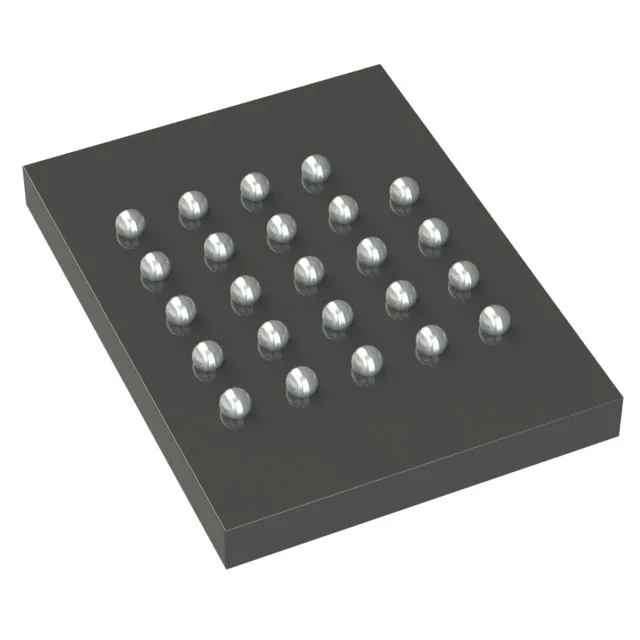
Infineon Technologies S25FL256SAGBHIA03 — Memory (DRAM / SRAM / Flash / EEPROM)

S25FL256SAGBHIA03 256Mbit NOR Flash, SPI Quad I/O, 133 MHz

MPNS25FL256SAGBHIA03
Active

Infineon FL-S series NOR Flash, S25FL256SAGBHIA03, 256 Mbit (32M x 8), SPI Quad I/O interface, 133 MHz clock, 2.7-3.6 V supply, -40 to 85°C, 24-BGA (8x6 mm) package, Tape & Reel.

$5.3100Ref. price · indicative, final on quote
Packaging24-TBGA
RoHSROHS3 Compliant
SeriesFL-S
Independent supplier — new & surplus stockAuthenticity-screened · ESD-safe packingListing updated Aug 2026

Specifications

S25FL256SAGBHIA03 specifications
ParameterValue
SeriesFL-S
Memory typeNon-Volatile
MountingSurface Mount
Voltage2.7V ~ 3.6V
Frequency133 MHz
Memory interfaceSPI - Quad I/O
Operating temperature-40°C ~ 85°C (TA)
PackageTape & Reel (TR) Cut Tape (CT)
TechnologyFLASH - NOR
Memory size256Mbit
Memory formatFLASH
Case24-TBGA
Memory organization32M x 8

Product details

ROHS3 compliance is confirmed. For a production BOM, this part presents no imminent obsolescence risk; the supply channel is stable through standard distribution and independent sourcing.

This 256 Mbit density with Quad I/O at 133 MHz is a common choice for code storage in industrial controllers, networking gear, and FPGA configuration memories. If your design requires operation up to 105°C, the S25FL256SAGMFV000 (same density and speed, 105°C rated, Tray package) or the S25FL256SDSMFV013 (80 MHz, 105°C, Tape & Reel) are the temperature-upgraded alternatives within the same FL-S family. The S25FL256SAGBHI300 is a Tray-packaged sibling with otherwise identical ratings — the only difference is the shipping medium, not the silicon.

Frequently asked questions

What is the pinout of S25FL256SAGBHIA03?

The pinout is defined by the 24-ball BGA package. The datasheet provides the ball assignment map for the SPI Quad I/O signals (CS#, SCK, SI/SIO0, SO/SIO1, WP#/SIO2, HOLD#/SIO3) and supply/ground balls.