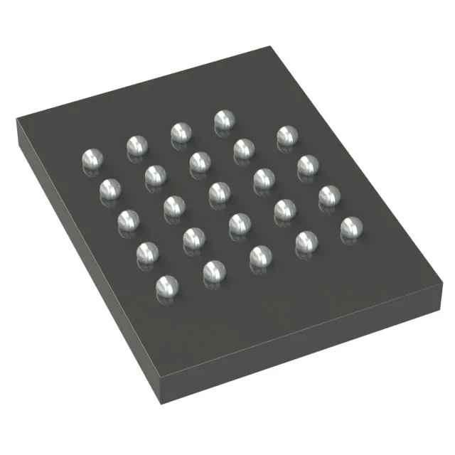
256 Mbit NOR Flash with Quad-SPI for industrial code storage
The 133 MHz clock on the Quad-SPI interface translates to a theoretical 532 Mbps read bandwidth when all four I/O lines are active. In practice, the controller latency and command overhead drop that to something closer to 400 Mbps, but it still boots a 32-bit MCU in under a millisecond from cold reset. The Quad-SPI protocol also supports Execute-in-Place (XIP), so the MCU can run code directly from the flash without shadowing to RAM — useful when the 256 Mbit density holds both the application image and a file system.
Industrial temperature range and BGA package realities
The 24-BGA package (8x6 mm) is a fine-pitch ball grid array — the reflow profile needs to match the solder ball alloy, and the board requires a stencil that aligns with the 0.8 mm ball pitch. The BGA footprint saves board area compared to an SOIC-16, but it also means the part is not hand-solderable without a rework station. For prototyping, the same die in a WSON package (S25FL256SAGBHI20) is a drop-in alternative if the layout can accommodate it.