It uses a SPI interface with Quad I/O and QPI support, allowing four-bit-wide data transfers at a clock frequency of 66 MHz.
66 MHz Quad SPI — throughput for fast boot and data logging
The 66 MHz clock rate with Quad I/O gives a theoretical read throughput of 264 Mbps (four bits per cycle). For a firmware-bringup engineer, this means the MCU can execute code directly from the Flash (XIP) with minimal wait states, provided the host controller supports Quad SPI. The QPI mode reduces the command overhead by using a four-bit address and data path, which helps when streaming large logs or OTA update images.
Active lifecycle — no imminent EOL risk
For a BOM cost engineer, this reduces single-source risk in the near term, though a second-source plan is always prudent for long-life designs.
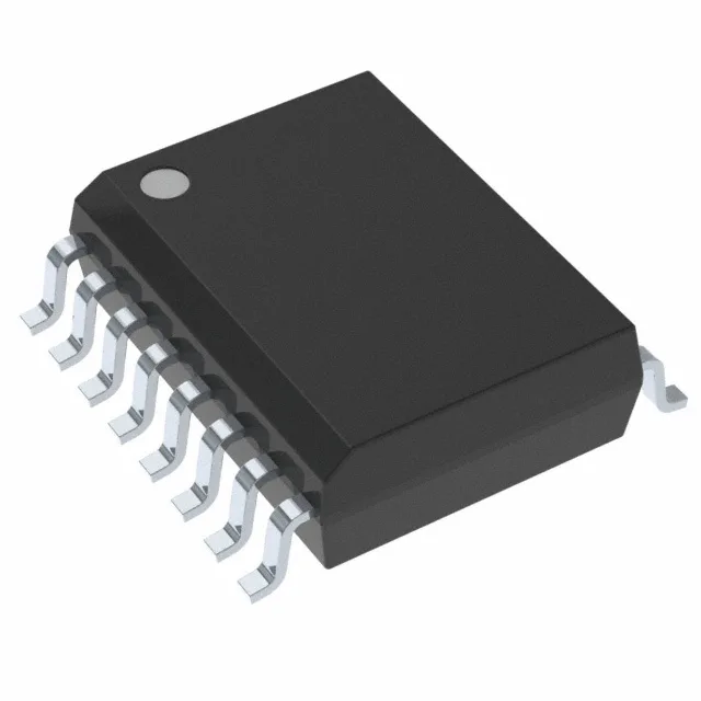
The surface-mount leads are Gull-wing style, inspectable and reworkable with standard soldering iron or hot air.