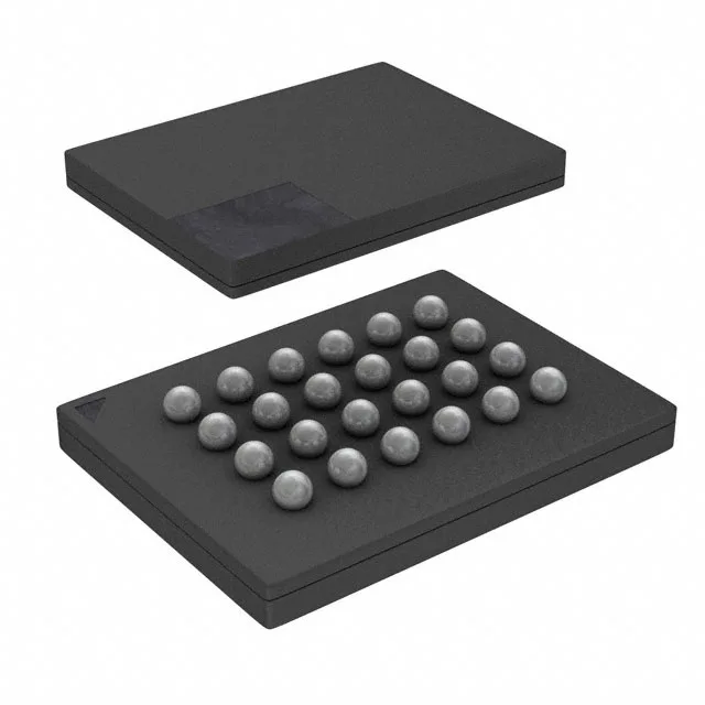
It uses a SPI interface with Quad I/O and QPI support for faster read and program operations, clocked at 66 MHz. The 24-TBGA package (6x8 mm) keeps the footprint compact for space-constrained designs.
If you are qualifying this for a production BOM, plan for a last-time-buy or a validated replacement.
66 MHz clock and Quad SPI — what the interface means for throughput
The 66 MHz clock rate with Quad I/O (four data lines) gives a theoretical peak read throughput of 264 Mbps (66 MHz x 4 bits). In practice, the controller overhead and command overhead reduce that, but it still offers a significant speed advantage over standard SPI at the same clock. The QPI mode allows the command and address to also use the four I/O lines, reducing instruction overhead. For a firmware engineer, this means faster code shadowing to RAM and quicker OTA update staging compared to a single-bit SPI NOR Flash running at the same frequency.
Package and temperature — design-in checklist
The 24-TBGA (6x8 mm) package is a fine-pitch BGA. The PCB layout needs a via-in-pad or microvia strategy for the inner balls; the datasheet's recommended land pattern should be followed exactly.