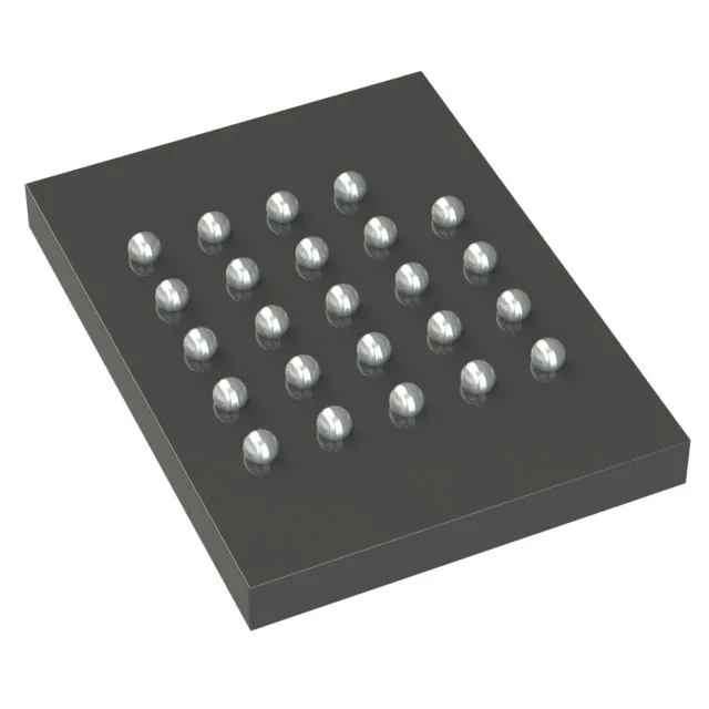
It uses a standard SPI interface with Quad I/O and QPI support, clocked at 66 MHz. It comes in a 24-ball TBGA package (8x6 mm) for surface-mount assembly. This is a non-volatile memory intended for code shadowing, data logging, and configuration storage in embedded systems where a serial NOR flash provides a good balance of density, read speed, and pin count.
66 MHz clock and Quad SPI — what the interface means for throughput
The 66 MHz clock frequency is the base rate for single-SPI reads. With Quad I/O, the effective throughput can reach 264 Mbps (66 MHz x 4 data lines), which is enough for fast firmware boot or streaming sensor data without needing a parallel bus. The QPI mode further reduces the command overhead by using the quad lines for address and command as well, which helps when the host controller supports it. For a design that needs to execute code in place (XIP) from flash, the 66 MHz speed keeps the CPU fed without wait states on many Cortex-M class MCUs running at similar clock rates.
Industrial temperature range — where this part runs reliably
This is not an extended-range part for under-hood or downhole use, but it handles the thermal cycling of a factory floor or a telecom cabinet without issue. The 24-BGA package has a small footprint (8x6 mm), which helps with board space, but the BGA requires careful PCB layout and X-ray inspection for solder joint quality in production.