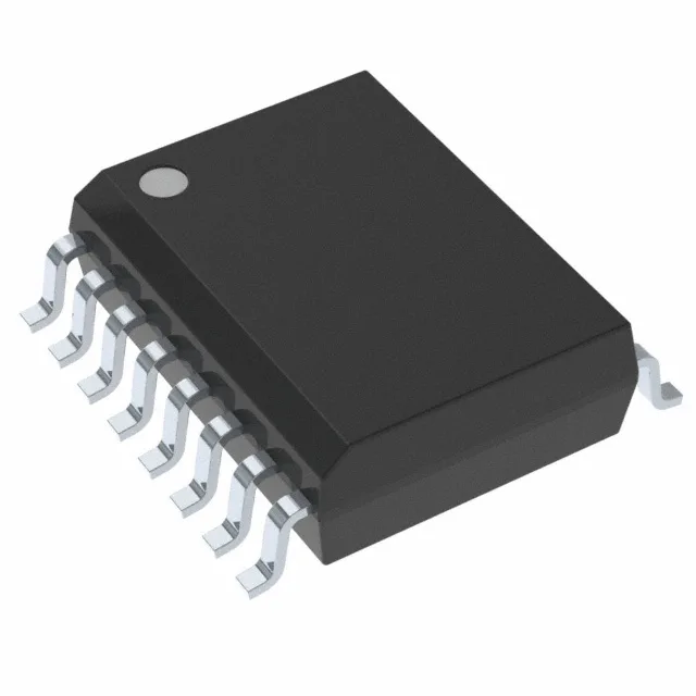
Infineon Technologies S25FL256LAGNFN010 — Memory (DRAM / SRAM / Flash / EEPROM)

S25FL256LAGNFN010 256Mbit NOR Flash, 133 MHz SPI

MPNS25FL256LAGNFN010
Active

Infineon FL-L series, S25FL256LAGNFN010, 256Mbit NOR Flash, SPI - Quad I/O, QPI, 133 MHz, 2.7V~3.6V, -40°C~125°C, 8-WDFN Exposed Pad (8-WSON 6x8), Tray.

$4.7500Ref. price · indicative, final on quote
Packaging8-WDFN Exposed Pad
StockContact for availability
MOQ1 pcs
  • 100% new & originalTraceable channels only — no refurbs, no pulls, no remarked parts.
  • Date & lot codes on quoteStated per line before you commit; label photos on request.
  • MSL-compliant ESD packingMoisture-sealed bags with indicator cards; reels photo-verified.
  • PayPal buyer protectionPay by T/T, PayPal or Payoneer — card payments covered end to end.

Specifications

S25FL256LAGNFN010 Technical Specifications
ParameterValue
SeriesFL-L
Memory typeNon-Volatile
Mounting typeSurface Mount
Voltage2.7V ~ 3.6V
Frequency133 MHz
Memory interfaceSPI - Quad I/O, QPI
Operating temperature-40°C ~ 125°C (TA)
PackageTray
TechnologyFLASH - NOR
Memory size256Mbit
Memory formatFLASH
Case8-WDFN Exposed Pad
Memory organization32M x 8

Product details

256 Mbit NOR flash for code and parameter storage

The Infineon S25FL256LAGNFN010 is a 256 Mbit NOR flash from the FL-L series, organized as 32M x 8. It communicates over SPI with Quad I/O and QPI support, clocking at 133 MHz. The 2.7 V to 3.6 V supply range and -40°C to 125°C operating temperature suit industrial and automotive environments. The 8-WSON (6x8 mm) package with exposed pad aids thermal transfer.

133 MHz Quad SPI — throughput for XIP and fast boot

The 133 MHz clock rate with Quad I/O delivers read throughput well above single-bit SPI, critical for execute-in-place (XIP) firmware and fast boot sequences in MCU and FPGA systems. The QPI mode reduces command overhead by using the same four I/O lines for address and data, which tightens bus turnaround in shared-SPI topologies.

Mounting and thermal interface

The 8-WSON package with exposed pad requires a thermal via pattern under the pad for effective heat sinking. The pad is electrically connected to ground (substrate); confirm isolation in your layout. The 6x8 mm footprint fits alongside QFN devices on the same reflow profile.

Frequently asked questions

Is S25FL256LAGNFN010 obsolete or active?

It is active in production. No end-of-life notification is in effect, so it is safe for new designs and ongoing production.

What is the memory size and organization of S25FL256LAGNFN010?

It is 256 Mbit organized as 32M x 8.

What is the clock frequency of S25FL256LAGNFN010?

The maximum SPI clock frequency is 133 MHz.

Where can I buy S25FL256LAGNFN010 and how do I get a price?

This part is sourced through independent distribution. Submit an RFQ for current availability and pricing — confirmed at quote time.