Active production — no end-of-life watch needed
The S25FL256LAGMFI003 carries an Active lifecycle status, meaning Infineon continues to manufacture and support this order code for new designs and production builds. It is ROHS3 compliant, so it clears the EU material-restriction gate without an exemption letter.
256 Mbit NOR flash with Quad SPI — throughput and pin count
Organised as 32M x 8 bits, the 256 Mbit density suits firmware images, calibration tables, and boot code that need fast random-access read and execute-in-place capability — the NOR array delivers single-cycle random access latency that NAND cannot match. The SPI interface supports Quad I/O and QPI protocols at a clock frequency up to 133 MHz, which lifts the read throughput to roughly 66 MB/s on a quad-lane bus — enough to shadow a full firmware image into RAM in under a second without saturating the SPI controller.
Industrial temperature grade and supply rail
Rated for -40 °C to 85 °C ambient (TA), this is the industrial temperature band — it covers outdoor telecom cabinets, factory-floor controllers, and automotive body electronics that do not sit under the hood. The supply range is 2.7 V to 3.6 V, which aligns with the common 3.3 V logic rail used by most MCUs and SoCs that boot from external SPI flash; no level translator is needed between the flash and a 3.3 V host.
16-SOIC wide-body — footprint and assembly
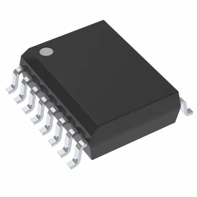
Housed in a 16-SOIC package with the standard 7.50 mm body width and 1.27 mm pin pitch, the S25FL256LAGMFI003 uses a surface-mount footprint compatible with reflow soldering and automated optical inspection — no hand-solder or press-fit step. The supplier device package is listed as 16-SOIC; the wide-body variant provides more clearance between adjacent pins than the narrow 3.90 mm SOIC, which reduces the risk of solder bridging during reflow and eases PCB routing between the flash pins and the host controller.