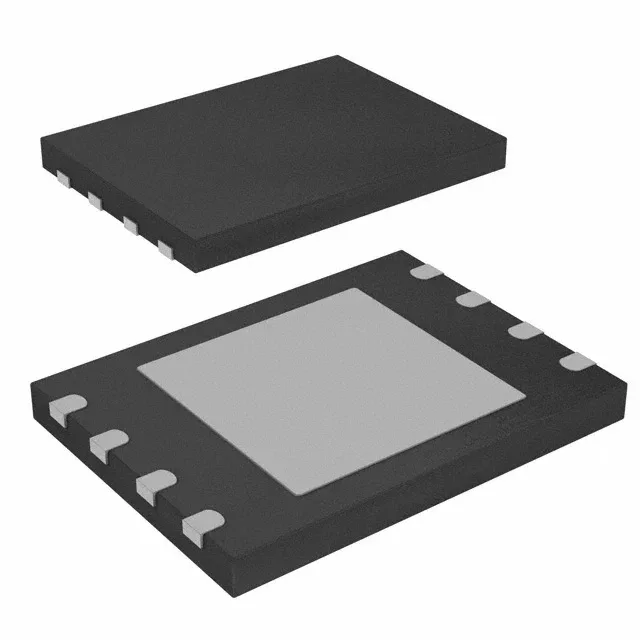
64 Mbit NOR Flash with automotive pedigree
It uses a standard SPI interface with Quad I/O support, clocked at up to 108 MHz for fast read throughput. The memory is organized as 8M x 8 bits and operates from a 2.7V to 3.6V supply rail.
For a 64 Mbit device, this means the entire memory can be read in under 80 ms at full speed — relevant for fast boot sequences in automotive ECUs or industrial controllers where the MCU's internal flash is insufficient.
This part carries AEC-Q100 stress qualification, making it suitable for automotive cabin and body electronics, as well as industrial environments that require the extended reliability screening. Note that under-hood or engine-bay applications requiring 105°C or 125°C ambient would need a different temperature grade variant.
Obsolete — sourcing reality for sustainment programs
The exposed thermal pad should be connected to a ground plane for heat dissipation, though at the 64 Mbit density and typical read currents the thermal demand is modest. The SPI interface uses standard CMOS-level signals, compatible with 3.3V logic families without level translation.