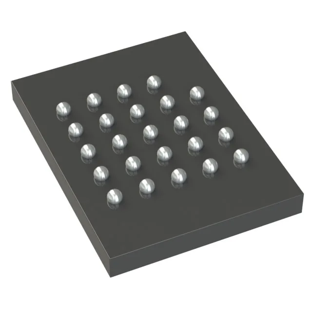
32Mbit NOR flash at 108 MHz — SPI Quad I/O for automotive
The S25FL132K0XBHB020 is a 32Mbit NOR flash from Infineon's FL1-K series, organized as 4M x 8 bits and accessed via a SPI Quad I/O interface running at 108 MHz. The Quad I/O reduces read latency by transferring four bits per clock cycle — at 108 MHz that's 54 MB/s theoretical throughput, enough to shadow-execute code from flash in many automotive MCU designs without a separate RAM footprint for the application image. AEC-Q100 qualification and a -40°C to 105°C operating range place this part in the under-hood and engine-bay temperature band — the flash array retains data through the thermal cycles of an automotive ignition-off to full-load drive cycle.
No official successor or pin-compatible replacement is recorded from the original manufacturer. For existing BOM positions that require this exact order code, supply is available through independent distribution — quantities are lot-specific and confirmed at RFQ. The 24-TBGA footprint (8x6 mm) is not shared by the active FL1-K siblings in different packages, so a board spin would be needed to migrate to a current-production part.
Package and board-fit — 24-TBGA 8x6 mm
The 24-ball TBGA package measures 8x6 mm with a 0.80 mm ball pitch typical of this density. The surface-mount footprint requires a solder-paste stencil aperture matched to the ball diameter for reliable reflow — the BGA's corner balls are the alignment fiducials during pick-and-place. No exposed thermal pad; the package's junction-to-board thermal path relies on the outermost balls and the PCB copper plane beneath the die shadow.