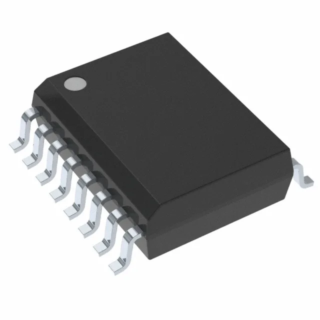
Infineon Technologies S25FL129P0XMFV003 — Memory (DRAM / SRAM / Flash / EEPROM)

Infineon S25FL129P0XMFV003 NOR Flash, 128Mbit, SPI Quad I/O

MPNS25FL129P0XMFV003
Obsolete

Infineon FL-P series NOR Flash, 128 Mbit, 16M x 8, SPI Quad I/O interface, 104 MHz clock, 2.7-3.6V supply, -40°C to 105°C, 16-SOIC (7.50mm Width), Tape & Reel.

$3.9734Ref. price · indicative, final on quote
Sourced new & surplus through independent channelsAuthenticity-screened · ESD-safe packingListing updated Jul 2026

Specifications

S25FL129P0XMFV003 specifications
ParameterValue
SeriesFL-P
Memory typeNon-Volatile
MountingSurface Mount
Voltage2.7V ~ 3.6V
Frequency104 MHz
Memory interfaceSPI - Quad I/O
Operating temperature-40°C ~ 105°C (TA)
PackageTape & Reel (TR)
TechnologyFLASH - NOR
Memory size128Mbit
Memory formatFLASH
Case16-SOIC (0.295\", 7.50mm Width)
Memory organization16M x 8
Write cycle time - word, page5µs, 3ms

Product details

128 Mbit NOR Flash for code storage — what the Quad SPI bus means for boot speed

The S25FL129P0XMFV003 is a 128 Mbit (16M x 8) NOR Flash from the FL-P series, organized for direct code execution or high-speed firmware shadowing. Its SPI Quad I/O interface at 104 MHz clock lets the controller read four bits per cycle — a 416 Mbps theoretical throughput that cuts boot time versus a standard SPI part running at the same clock. NOR Flash reads are fast enough to execute code in place (XiP) on many MCUs, so this part suits applications where the processor boots directly from flash without copying to RAM. The 5 µs word write and 3 ms page write cycle times mean field firmware updates are practical but budget the page erase time into the update window.

Industrial temp grade and supply — where this part fits on the board

Housed in a 16-SOIC wide-body (7.50 mm width) package, the part reworks cleanly with a hot-air station — the 0.295-inch body gives enough clearance for a nozzle to reach all pins without cooking adjacent components. Pin 1 is marked with a dot on the package top; the wide SOIC footprint is standard enough that a replacement part from another vendor often lands on the same pads without a board spin.

Obsolete — sourcing reality for a discontinued NOR Flash

For a BOM that already qualifies this footprint and interface, the procurement path is to request a quote against the required quantity. Availability and pricing vary by lot — the part is sourced to order, not held in ready inventory. If the design can tolerate a package change, a current-production NOR Flash in a different package may be a lower-risk long-term option, but that requires a board layout revision.

Frequently asked questions

Does the S25FL129P0XMFV003 work on a 3.3 V nominal rail without extra regulation?

The 2.7–3.6V supply range covers a 3.3 V nominal rail within normal tolerance. Standard SPI FLASH decoupling — typically 100 nF per VCC pin, placed close to the device — is sufficient. The 2.7 V minimum is the constraint to watch under brown-out; confirm your rail stays above it during all operating states if the application is safety-critical.

Does the 3 ms page write cycle time meet typical boot-time budgets for a PLC firmware load?

A 3 ms page write is routine for SPI NOR flash; the limiting factor for boot time is usually the SPI clock rate and the flash-to-memory-controller transfer mode rather than the write time itself (which applies during programming, not boot-read). If the design uses XIP (execute-in-place) the clock frequency of 104 MHz matters more than the write timing. Confirm the MCU's Quad SPI controller is configured for the 104 MHz interface speed the part supports.