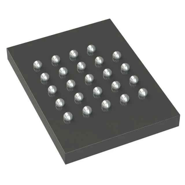
Infineon Technologies S25FL129P0XBHV203 — Memory (DRAM / SRAM / Flash / EEPROM)

S25FL129P0XBHV203 128Mbit NOR Flash, Quad-SPI, 104 MHz

MPNS25FL129P0XBHV203
Obsolete

Cypress FL-P series, S25FL129P0XBHV203, 128Mbit NOR Flash, SPI - Quad I/O, 104 MHz, 2.7V-3.6V, -40°C to 105°C, 24-TBGA (8x6mm), Tape & Reel.

Sourced new & surplus through independent channelsAuthenticity-screened · ESD-safe packingListing updated Jul 2026

Specifications

S25FL129P0XBHV203 specifications
ParameterValue
SeriesFL-P
Memory typeNon-Volatile
MountingSurface Mount
Voltage2.7V ~ 3.6V
Frequency104 MHz
Memory interfaceSPI - Quad I/O
Operating temperature-40°C ~ 105°C (TA)
PackageTape & Reel (TR)
TechnologyFLASH - NOR
Memory size128Mbit
Memory formatFLASH
Case24-TBGA
Memory organization16M x 8
Write cycle time - word, page5µs, 3ms

Product details

If your BOM still references this order code, the procurement decision is whether to qualify a replacement or source remaining inventory through distribution that can trace stock provenance.

128 Mbit NOR Flash with Quad-SPI at 104 MHz

This is a 128 Mbit (16M x 8) NOR Flash memory from Cypress's FL-P series, organized as 16M x 8 bits. It uses an SPI interface with Quad I/O support, meaning it can transfer four bits per clock cycle, and is rated for a clock frequency of 104 MHz. That combination delivers read throughput sufficient for XiP (eXecute-in-Place) code storage in embedded systems where a separate RAM cache is not available. The memory is non-volatile NOR Flash, which provides fast random-read access and byte-rewrite capability, making it suitable for firmware storage, configuration data, and boot code in industrial and telecom equipment.

The supply voltage range of 2.7V to 3.6V aligns with standard 3.3V logic rails. It comes in a 24-ball TBGA package measuring 8x6 mm (supplier device package 24-BGA). The Tape & Reel (TR) packaging is the shipping medium, not the device case.

Write-cycle timing and endurance context

Page write time is 3 ms typical, and word write time is 5 µs. These figures matter when sizing the firmware update window: a full 128 Mbit erase-and-write cycle takes longer than the page write suggests, because NOR Flash requires a sector erase before programming. Plan for the erase granularity when designing OTA or field-update routines.

Frequently asked questions

What is the replacement for S25FL129P0XBHV203?

For a pin-compatible alternative, look at other members of the Cypress FL-P family with the same 24-TBGA footprint and Quad-SPI interface, such as the S25FL128S series, but verify the exact density and voltage range against your BOM. A cross-reference search through distribution may identify a drop-in replacement.

Is S25FL129P0XBHV203 compatible with SPI?

Yes, it uses a standard SPI interface with Quad I/O support. The memory interface is SPI - Quad I/O, meaning it is backward-compatible with single-bit SPI but can also operate in four-bit mode for higher throughput at the 104 MHz clock rate.

Where to buy S25FL129P0XBHV203?

Because this part is obsolete, it is not available through authorized factory channels. It can be sourced through independent distributors and brokers who carry surplus inventory. Submit an RFQ for current availability and pricing — stock and price are confirmed at quote time, not on a public listing.