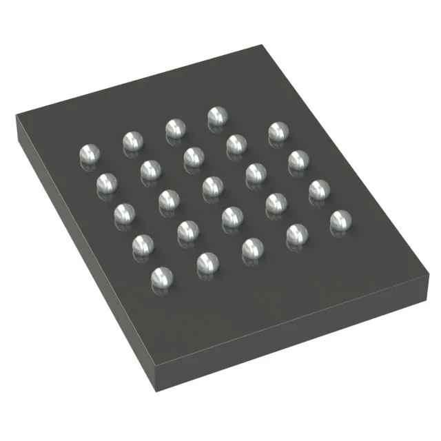
128 Mbit Quad-SPI NOR Flash — 24-BGA, obsolete
It reads at up to 104 MHz over the Quad-SPI interface, suiting code-shadowing, execute-in-place, and fast firmware staging in embedded systems.
Quad-SPI at 104 MHz — throughput and bus margin
The 104 MHz clock rate over the Quad I/O interface delivers a sustained read throughput that keeps the host processor fed without stalling. For a 128 Mbit density, the page program time is 3 ms and the word write cycle is 5 µs, which matters when sizing the OTA staging area or config-block update window.
24-BGA footprint — layout and rework notes
The 24-BGA (8x6 mm) package is a fine-pitch ball-grid array requiring a solder-paste stencil matched to the ball diameter and a reflow profile per JEDEC. No exposed thermal pad, so dissipation relies on the PCB copper plane under the BGA.