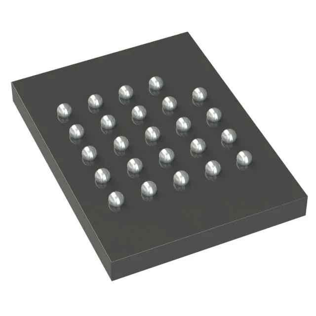
It uses a Quad SPI interface (SPI - Quad I/O) clocked at 66 MHz, which gives a read throughput high enough for execute-in-place (XIP) code shadowing or fast firmware boot in embedded systems. Packaged in a 24-ball TBGA (8 mm x 6 mm), it suits space-constrained designs where a small footprint matters.
The 66 MHz clock frequency on the Quad I/O interface delivers a raw bit rate of 264 Mbps (66 MHz x 4 I/Os). For a firmware engineer, this means the part can sustain fast code shadowing into RAM or even direct XIP with acceptable latency, depending on the system bus speed. The SPI - Quad I/O interface is backward-compatible with standard SPI, so a legacy controller that only supports single-bit SPI will still work, but you leave three-quarters of the throughput on the table. If your MCU has a Quad SPI peripheral, enable it — the difference in boot time is measurable.
The 24-TBGA (8x6) package is a fine-pitch BGA — the rework lab should verify the ball layout against the board footprint before stenciling; the supplier device package code is 24-BGA (8x6). Surface-mount only, no through-hole option.
That means no last-time-buy clock is ticking, and the part is eligible for new designs. No planned obsolescence risk on this code today.