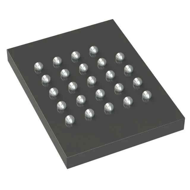
128 Mbit NOR Flash in a 24-ball BGA
The S25FL128SDPBHV210: It communicates over a Quad SPI interface at up to 66 MHz, giving the host controller fast read and program access for code shadowing, data logging, or over-the-air update staging. The 24-ball TBGA (8x6 mm) package is a fine-pitch BGA. The hidden solder joints mean X-ray inspection is the norm during first-article build.
The 66 MHz clock rate on the Quad SPI interface delivers a theoretical peak throughput around 33 MB/s in quad-read mode. That is fast enough to support XiP (eXecute-in-Place) from the Flash for many embedded applications, provided the MCU's QSPI controller and cache architecture can keep the pipeline fed. Real-world throughput depends on the controller's command overhead and the number of wait states inserted during the initial access latency — budget for 25-30 MB/s sustained in a well-tuned system. The SPI interface is Quad I/O, meaning four data lines plus a clock and chip-select. That cuts the pin count compared to a parallel NOR Flash, freeing up GPIOs on the host. The trade-off is that the QSPI controller on the MCU side needs to support the quad-read command set (usually 0xEB or 0x6B opcodes) to benefit from the four-lane read.
BGA footprint and assembly considerations
The 24-BGA (8x6 mm) package uses a 0.8 mm ball pitch, which is within the capability of standard SMT lines. The stencil aperture for the balls should be about 0.4 mm diameter with a 0.125 mm thickness to get good solder paste volume without bridging. The package is MSL 3 out of the bag — if the moisture-barrier bag has been open longer than the floor-life window, bake the parts at 125°C for 24 hours before reflow to avoid popcorning. Because the solder joints are under the package, visual inspection is not possible. X-ray inspection during first-article build is the standard practice to catch head-in-pillow or non-wet opens. The 8x6 mm body is small enough that it does not need an underfill for most shock and vibration profiles, but if the board sees high-g environments, a corner-bond adhesive adds margin.
The FL-S family has broad market adoption, so supply through the independent channel is steady. The base product number is S25FL128, which covers the full 128 Mbit FL-S family across package and temperature variants. If a future design needs a different package or wider temperature range, the migration stays within the same die family, minimising firmware re-qualification.