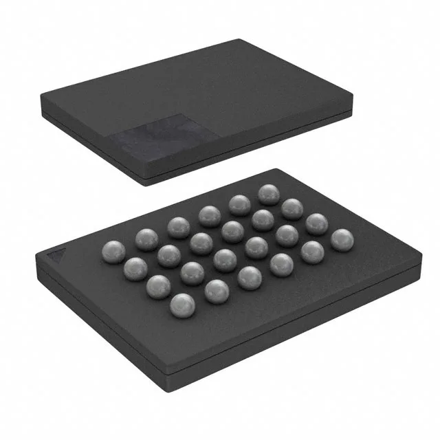
Automotive-grade NOR Flash in a 6x8 BGA
The 24-TBGA package measures 6x8 mm, a compact footprint suited for space-constrained automotive ECUs, ADAS modules, and telematics control units where non-volatile code or data storage is needed over the -40 to 105 °C temperature range.
The 66 MHz clock rate with Quad I/O (four data lines) gives a sustained read throughput that can feed an automotive MCU's execute-in-place (XIP) or shadow-to-RAM boot flow without stalling the core. If your application uses the SPI bus for firmware shadowing or over-the-air update staging, the 66 MHz Quad I/O keeps the transfer window short. The same interface is backward-compatible with single and dual SPI, so it drops into an existing SPI Flash socket without firmware changes — you just leave the extra pins unconnected if the host doesn't support Quad.
The AEC-Q100 qualification and -40 to 105 °C operating temperature tell you this part was characterised for the thermal cycling and reliability demands of automotive under-hood and chassis domains. For industrial or outdoor telecom designs that don't require the full AEC paperwork, the temperature range alone still covers most extended-environment cases.
24-TBGA footprint — rework and inspection considerations
Solder joints are not visually inspectable — X-ray is the standard for void and alignment check. If your rework station doesn't have a pre-heater and a hot-air nozzle sized for this body, the adjacent passives can shift during removal.
The base product number S25FL128 covers a family of density and package variants; if your procurement team wants a second-source hedge, the S25FL128SDPBHA303 (same die, different package code) is a direct replacement candidate — confirm the package suffix matches your footprint before swapping.