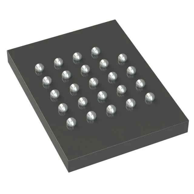
128 Mbit NOR flash for automotive firmware storage
The S25FL128SDPBHB210 is a 128 Mbit NOR flash from Infineon's FL-S series, organized 16M x 8 and accessed over an SPI Quad I/O interface clocked at 66 MHz. The Quad I/O read reduces the instruction overhead — four data lines per clock cycle instead of one — so the effective throughput for code shadowing or parameter logging lands well above a single-bit SPI part at the same clock rate. NOR flash is the right choice here: random-access read with fast page fetch means the MCU can execute code directly in place (XIP) without copying a bootloader to RAM first. The 128 Mbit density fits a full firmware image plus a redundant bank for over-the-air update staging in an automotive ECU.
Temperature grade and AEC-Q100 qualification
The 105°C ceiling gives margin above the 85°C cabin-grade limit, so the flash retains data retention specs when the ECU sits near a hot exhaust manifold or turbocharger. AEC-Q100 qualification means the part passed the full stress suite: high-temperature operating life (HTOL), temperature cycling, ESD (HBM/CDM), latch-up, and early-life failure rate (ELFR) screening. For a production ECU BOM, that certification replaces the need for a separate qualification run.
Package and board-fit for the 24-TBGA
The BGA footprint demands a solder-paste stencil aperture matched to the ball diameter — a 0.40 mm aperture with 0.45 mm pad diameter keeps the solder joint height within the 0.20–0.30 mm range for reliable second-level interconnect after reflow. No external level translator needed for the SPI bus if the host MCU also runs at 3.3V.
No official second-source or pin-compatible cross-reference is listed on the manufacturer record.