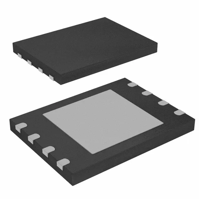
The Infineon S25FL128SAGNFI010 is a 128 Mbit (16M x 8) NOR Flash memory from the FL-S family, built for code-shadowing and data-logging in embedded systems that need fast, reliable non-volatile storage. Its SPI Quad I/O interface clocks at 133 MHz, so reading four bits per cycle gives an effective throughput that keeps a Cortex-M or RISC-V core fed without stalling on flash wait states.
Active production — no LTB scramble yet
No last-time-buy notice, no end-of-life letter to chase. The FL-S series has been a workhorse in the NOR Flash space for years, and Infineon continues to support it alongside the newer SEMPER and EXCELON families for higher-density or automotive-grade needs.
Quad I/O vs plain SPI — the throughput difference
Standard SPI shifts one bit per clock on a single data line; Quad I/O uses four data lines simultaneously. At 133 MHz, that's 532 Mbit/s raw read bandwidth versus 133 Mbit/s for single-SPI. For a 128 Mbit part, a full-chip read at Quad I/O takes about 240 ms — the same operation over single-SPI would push past a second. The trade-off is four extra signal traces on the board, but the pin count is still an 8-pin package (8-WSON), so the routing overhead is minimal.
Package and rework — the 8-WSON exposed pad
The S25FL128SAGNFI010 comes in an 8-WDFN exposed pad package (supplier device package 8-WSON, 6x8 mm). For rework, WSON packages are friendlier than QFN: the leads are visible at the edges, so hot-air removal and replacement with a fine-tip iron is feasible.