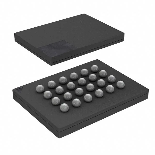
Infineon Technologies S25FL128SAGBHVB00 — Memory (DRAM / SRAM / Flash / EEPROM)

S25FL128SAGBHVB00 128Mbit NOR Flash, 133 MHz Quad-SPI

MPNS25FL128SAGBHVB00
Active

Infineon FL-S series S25FL128SAGBHVB00, 128Mbit NOR Flash, 133 MHz SPI - Quad I/O, 2.7V~3.6V, -40°C~105°C, 24-TBGA (6x8 mm), Tray.

$3.8387Ref. price · indicative, final on quote
Sourced new & surplus through independent channelsAuthenticity-screened · ESD-safe packingListing updated Aug 2026

Specifications

S25FL128SAGBHVB00 specifications
ParameterValue
SeriesFL-S
Memory typeNon-Volatile
MountingSurface Mount
Voltage2.7V ~ 3.6V
Frequency133 MHz
Memory interfaceSPI - Quad I/O
Operating temperature-40°C~105°C(TA)
PackageTray
TechnologyFLASH - NOR
Memory size128Mbit
Memory formatFLASH
Case24-TBGA
Memory organization16M x 8

Product details

The S25FL128SAGBHVB00: It communicates over a Quad-SPI interface at up to 133 MHz, which means the controller can read four bits per clock cycle — delivering the throughput needed for execute-in-place (XIP) code shadowing or high-speed data logging without a parallel bus.

Quad-SPI at 133 MHz — timing margin and bus throughput

At 133 MHz in Quad-I/O mode the part delivers a sustained read throughput that keeps a Cortex-M or RISC-V core fed without wait states on the code bus. The SPI clock is the spec that determines whether your firmware boots fast enough and whether the OTA staging area can be read back within the radio's duty-cycle window. Design the PCB trace length-matched and keep the clock line short — the 133 MHz edge rate is fast enough that a few centimetres of uncontrolled impedance will eat into setup/hold margin.

Industrial temperature range — deployment envelope

The 105°C ceiling covers most industrial and automotive cabin applications; if your system sees sustained junction temperatures above that, you need a higher-grade part. The BGA package (6x8 mm) keeps the footprint small, but the BGA demands a controlled reflow profile and post-solder X-ray inspection — plan for that in your assembly process.

There is no last-time-buy clock ticking, and Infineon has not announced a successor. The base product number S25FL128 covers multiple package and temperature variants; the BHVB00 suffix identifies this specific BGA, industrial-tray option.

Frequently asked questions

Is S25FL128SAGBHVB00 compatible with standard SPI?

Yes, it supports standard SPI in addition to Dual and Quad I/O modes. The Quad-SPI interface is backward-compatible: you can drive it with a standard single-bit SPI master and read one bit per clock, or switch to Quad mode for higher throughput. The 3.3 V supply rail is standard for most SPI NOR Flash designs.

Does S25FL128SAGBHVB00 have a datasheet?

Yes, the full datasheet for the S25FL128S FL-S series is available from Infineon. It covers the Quad-SPI protocol details, timing diagrams, erase/program times, and the complete instruction set. The datasheet is the authoritative source for AC timing parameters and the recommended reflow profile for the 24-BGA package.

Is S25FL128SAGBHVB00 compatible with 3.3V SPI?

The I/O pins are 3.3 V tolerant and the Quad-SPI interface signals are referenced to VCC.