This combination makes it suited for execute-in-place (XIP) code storage, firmware updates, and data logging in embedded systems where fast random-access read performance matters.
133 MHz and Quad I/O — read throughput for boot and XIP
The 133 MHz clock rate with Quad I/O yields a theoretical maximum read throughput of 532 Mbps (133 MHz x 4 lines). In practice, the controller overhead and command overhead reduce this, but it still provides a significant margin over single-bit SPI at the same frequency. For a processor booting from this Flash, the Quad I/O mode reduces the time to load the first instruction block compared to a two-wire interface.
The wide operating range means the Flash retains data integrity and read timing margins across thermal cycling common in motor drives, outdoor telecom, and engine bay electronics. The 2.7V to 3.6V supply range aligns with common 3.3V logic rails, with margin for brownout conditions.
24-ball BGA — footprint and reflow considerations
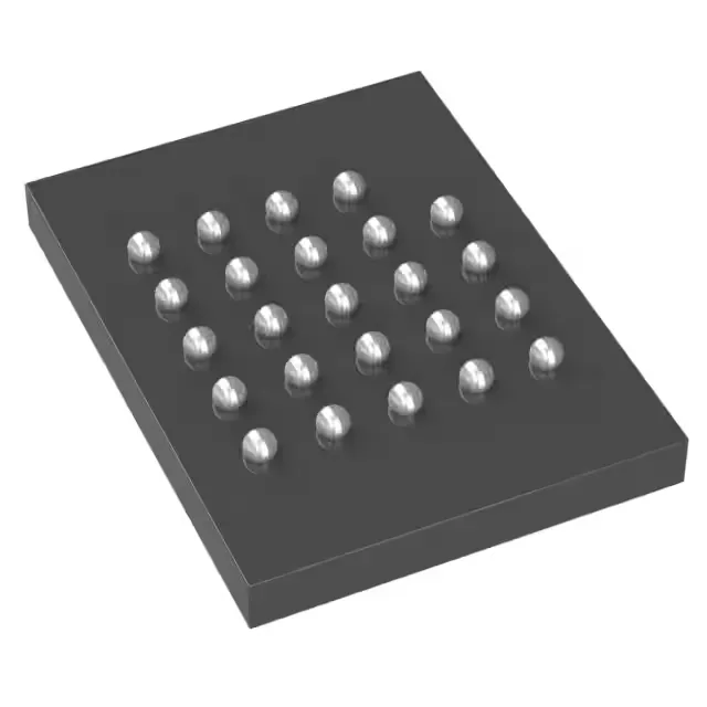
The 24-TBGA package measures 8x6 mm (supplier device package 24-BGA). The balls are on a fine pitch, so PCB layout must route signals cleanly under the package without via-in-pad unless filled and plated.