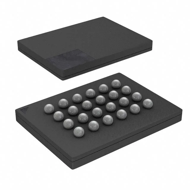
The S25FL128SAGBHI310 is a 128 Mbit (16 M x 8) NOR Flash memory from the Infineon (formerly Cypress) FL-S series, organized as 16M x 8 bits. It uses a Quad I/O SPI interface clocked at 133 MHz, which gives you a practical read throughput well beyond what a single-bit SPI can deliver — useful for code shadowing, execute-in-place (XIP) on a companion MCU, or storing configuration tables that need fast random access.
Quad SPI at 133 MHz — real throughput and layout considerations
The Quad I/O interface (four data lines plus clock and chip-select) at 133 MHz delivers a theoretical peak of 532 Mbps. In practice, the read command overhead and the initial access latency mean sustained throughput is lower, but it still beats a standard SPI NOR by a factor of four for sequential reads. This matters when the flash is the primary code store and the CPU boots directly from it — the faster read cuts boot time. At 133 MHz, signal integrity on the BGA layout becomes a concern. Keep the SPI traces length-matched within a few millimetres, avoid vias on the clock line if possible, and place a 10-22 ohm series resistor near the source on the clock output to damp reflections.
For a production BOM, this means you are not forced into a bridge-buy or a redesign cycle in the near term. The FL-S series is a mature, widely deployed NOR Flash family with good second-source optionality across the 128 Mbit density tier.
BGA rework and handling notes
Reballing is possible with a stencil and 0.3 mm solder spheres, but the fine pitch (0.8 mm) means careful alignment. Hot-air rework stations with a bottom preheater are preferred; hand soldering is not practical. After reflow, X-ray inspection of all 24 balls is the standard check for head-in-pillow or bridging.