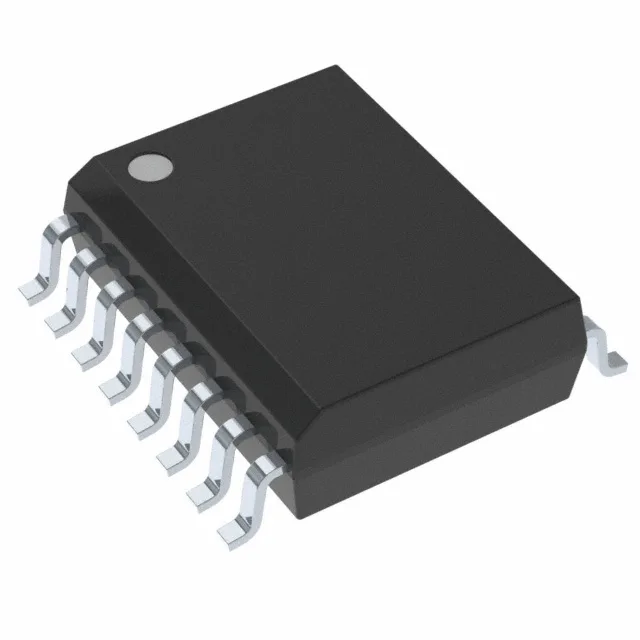
It uses a SPI interface with Quad I/O and QPI support, clocked at 66 MHz. Typical applications include firmware storage, boot code, configuration data, and parameter logging in embedded systems, industrial controllers, networking gear, and telecom infrastructure where a reliable, high-speed serial NOR Flash is needed.
66 MHz Quad I/O — what the clock speed means for read throughput
The 66 MHz clock frequency is the maximum SPI clock for Quad I/O reads. With four data lines active, the effective read throughput reaches about 264 Mbps (66 MHz × 4 bits), which is enough for fast code shadowing or high-speed data logging without needing a parallel NOR. The QPI mode reduces the command overhead by using the same four lines for address and command, trimming latency on random reads. For designs that currently run a single-SPI NOR at lower clock rates, moving to this part can cut firmware load times significantly without a PCB redesign — the 16-SOIC footprint and 3.3V supply keep the migration simple.
For a BOM planner, this removes the urgency to qualify a second source or stockpile for an impending EOL.
Package and supply — what to check on the board
The supply range of 2.7V to 3.6V means it runs directly from a 3.3V rail without an external regulator, but check that the rail stays above 2.7V during brown-out or cold-crank — if the supply dips below that, the memory may not retain data reliably during a write cycle. The industrial temperature grade covers most indoor and outdoor enclosures, though for extended automotive or downhole applications you would look at the automotive-grade siblings in the FL-L family.