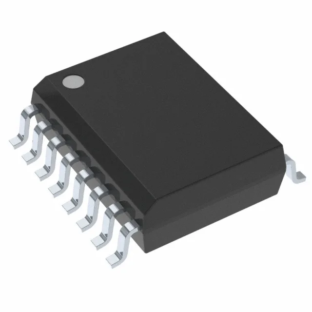
It communicates over a SPI bus with Quad I/O and QPI protocol support, clocked at up to 133 MHz.
133 MHz Quad SPI — what the clock rate buys you
A 133 MHz SPI clock with Quad I/O delivers a theoretical read throughput of 532 Mbps (four data lines × 133 MHz). In practice, execute-in-place (XIP) code shadowing from this part keeps up with many Cortex-M and RISC-V cores without a separate RAM staging area. The QPI mode reduces the command overhead by switching the bus to a full quad protocol after the initial instruction, which matters when the MCU fetches small, scattered code blocks rather than streaming large data sets. If the host controller lacks a Quad SPI peripheral, the part also supports standard single-bit SPI at the same clock rate, though throughput drops to 133 Mbps.
Supply and temperature — the operating envelope
The 2.7 V minimum supply lets this part run from a 2.8 V or 3.0 V rail without a boost regulator, which simplifies BOM on battery-powered edge nodes. The 3.6 V maximum is standard for 3.3 V systems with ±10% tolerance. The 16-SOIC package is a through-hole-compatible surface-mount footprint that reflows on standard profiles and is hand-solderable for prototypes.
Infineon continues to manufacture the FL-L series as a mainstream serial NOR Flash family.