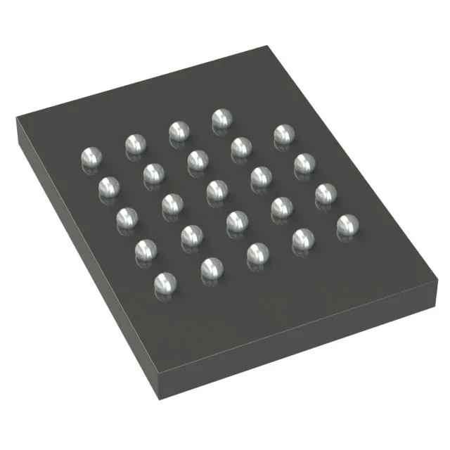
The S25FL128LAGBHV023: The 24-ball BGA (8x6 mm) footprint (supplier device package 24-BGA) demands a four-layer PCB for clean fan-out of the SPI and QPI signals — the 0.80 mm ball pitch leaves room for one via per signal between balls, but the inner rows require microvias or a dog-bone breakout. Supply decoupling should follow the reference design: a 100 nF ceramic placed within 2 mm of each VDD ball, with a 10 µF bulk cap per voltage plane.
Read throughput and interface
At 133 MHz clock, the Quad I/O interface delivers a theoretical 532 Mbit/s read throughput — enough to shadow a 128 Mbit code image into RAM in under 250 ms. The QPI mode reduces the command overhead by keeping the address and data on the same four I/O lines, which simplifies the controller state machine. The 16M x 8 organization means the device is byte-addressable on the SPI bus; the controller issues a 24-bit address for each read or write operation. For firmware-over-the-air updates, the 128 Mbit capacity holds two full application images plus a bootloader with room for a configuration sector.
Temperature grade and deployment
The 105°C ceiling gives 20°C margin above the standard industrial grade — critical for designs that must survive a hot-day stall condition. Active lifecycle status means no last-time-buy risk for ongoing production. The FL-L series is Infineon's current-generation SPI NOR family, so new designs can commit to this part without a near-term migration plan.