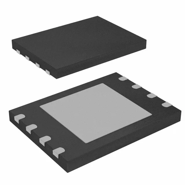
What this 128 Mbit NOR Flash delivers for your firmware and data storage
The S25FL127SABNFI103 is a 128 Mbit NOR Flash from Infineon's FL-S series, organised as 16M x 8 bits and accessed through a SPI Quad I/O interface running at 108 MHz. That clock rate, combined with the Quad I/O mode, pushes the effective read throughput well above what a single-bit SPI bus can sustain at the same frequency — a practical advantage when your MCU boots from external flash or logs data at high speed.
At 108 MHz in Quad I/O mode, the S25FL127SABNFI103 can deliver around 54 MB/s sustained read throughput (108 MHz × 4 bits) before protocol overhead. That bandwidth is enough to feed a Cortex-M7 or a mid-range FPGA configuration engine without stalling the core on instruction fetches. The SPI Quad I/O interface uses four I/O lines for data, reducing the pin count compared to a parallel NOR flash while still offering a significant speed-up over single-SPI. If your MCU or SoC has a Quad SPI controller, this part lets you keep the PCB routing simple — just four signal traces plus chip select and clock.
That said, NOR Flash supply can tighten during industry-wide memory allocation cycles — lead times stretch when foundry capacity shifts to higher-margin products.
Package and board-level integration
The supply voltage range is 2.7V to 3.6V, so a 3.3V rail with ±5% tolerance stays well within the window. Decoupling should follow the datasheet recommendation — a 100 nF ceramic close to each VCC pin, plus a bulk capacitor on the rail.