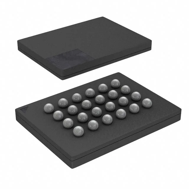
24-BGA footprint — layout notes
The 24-TBGA package measures 6x8 mm (supplier device package 24-BGA). This is a fine-pitch BGA — routing the Quad-SPI signals (CS#, CLK, IO0–IO3) out of the inner balls typically requires microvias or via-in-pad on a four-layer board. The 108 MHz clock edge is fast enough that signal integrity matters: keep the trace length matched within 10 mm between the Flash and the host controller, and place a 10–22 Ω series resistor close to the source on the clock line to damp reflections.
Firmware bring-up with Quad-SPI
When bringing up a board with this Flash, the Quad-SPI controller on the host MCU must be configured for the correct dummy cycles and read command (0xEB for Quad I/O fast read). The 108 MHz clock may require adjusting the drive strength on the Flash side — the FL-S series has configurable output driver strength via a nonvolatile register. If the first read returns garbage, check that the hold/reset pins are properly pulled high; an unconnected HOLD# pin floats and can glitch the bus.