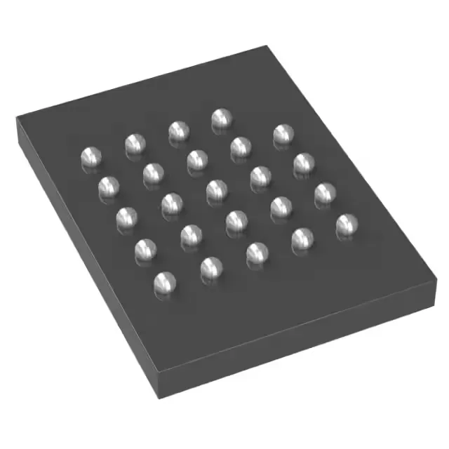
128 Mbit NOR Flash for code and data storage
The memory interface supports standard SPI, Dual I/O, and Quad I/O modes, allowing designers to balance pin count against read bandwidth. Quad I/O at 108 MHz provides a theoretical throughput of 54 MB/s, sufficient for high-performance MCUs and FPGAs that cache instructions from external flash.
Industrial temperature range and BGA footprint
The 24-ball BGA package (8 mm x 6 mm body) saves board area but requires careful PCB layout: controlled-impedance traces for the SPI lines, adequate decoupling near the supply balls, and a solder profile that meets the BGA reflow specification. The mounting is surface-mount only. The 24-TBGA package has a 0.8 mm ball pitch typical of this density class. Rework requires a hot-air station with a fine nozzle and preheat from the bottom; moisture sensitivity level should be verified before reflow if the original bag seal is broken.
The S25FL127SABBHVC03 is marked obsolete by the manufacturer. Because the part is obsolete, buyers should qualify a drop-in replacement or alternate source for new designs. The FL-S family has several density and speed variants, but the 24-BGA footprint and Quad SPI interface narrow the field. A cross-reference search against similar 128 Mbit NOR Flash parts in the same package is recommended for dual-sourcing or lifecycle extension.