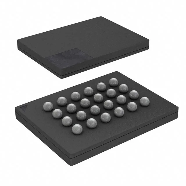
It is a non-volatile memory device intended for code shadowing, firmware storage, configuration parameter retention, and data logging in embedded systems.
New designs should not target this order code. For existing BOM lines, availability is limited to surplus and broker-channel inventory. No last-time-buy window remains open.
108 MHz Quad I/O — read throughput for XIP and fast boot
The Quad I/O SPI interface at 108 MHz delivers read throughput sufficient for execute-in-place (XIP) code execution from the Flash, reducing the need for a separate SRAM or DRAM for firmware shadowing. The 3 ms page write cycle time (word/page) is typical for this NOR generation and sets the expectation for firmware update latency — over-the-air updates or field reprogramming need to budget for this write speed across the 16 Mbit array.
24-ball BGA footprint and supply range
Housed in a 24-TBGA (6x8 mm) package, this part demands careful PCB layout for the BGA balls — the 0.8 mm pitch is manageable with standard assembly processes, but the BGA requires a solder-paste stencil and X-ray inspection for voiding. The supply voltage range of 2.7V to 3.6V aligns with common 3.3V logic rails, though the lower end accommodates 2.8V or 3.0V systems without a separate regulator.