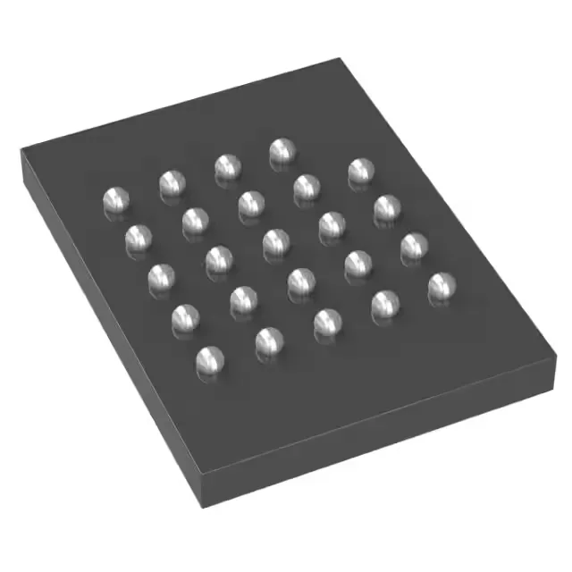
16 Mbit NOR flash in a 24-BGA — what the BGA means for the board
The S25FL116K0XBHV023 is a 16 Mbit NOR flash memory from the Infineon FL1-K series, organized as 2M x 8 bits. It uses the SPI Quad I/O interface, which clocks at up to 108 MHz — the quad-lane read effectively delivers four bits per clock cycle, so the sustained throughput for code shadowing or execute-in-place is higher than a standard single-lane SPI part at the same frequency. The 24-TBGA package (8x6 mm body, 24-BGA) has a 0.80 mm ball pitch — a four-layer PCB is the practical minimum for fan-out on the inner balls.
Obsolete — sourcing through surplus and last-time-buy channels
Infineon lists the S25FL116K0XBHV023 as obsolete. The base product number S25FL116 covers the 16 Mbit density in the FL1-K family; active variants in the same family may share the same pinout and protocol but differ in package or temperature grade — confirm the BGA footprint and operating range before substituting. Quantities are lot-specific and date-code dependent — a sealed reel with consistent date-codes from a single production run is the preferred condition.
Quad I/O read performance and the page write timing
The 108 MHz clock rate applies to the quad-I/O read command — the actual throughput depends on the initial command overhead (one byte for the instruction, three bytes for the address, one mode byte) before the data lanes switch to output. Once in continuous read mode, subsequent addresses skip the command byte, so sequential reads sustain near the full 54 MB/s theoretical peak (108 MHz × 4 bits). Page write cycle time is 3 ms typical for a 256-byte page. This is the NOR flash norm — the erase-before-write architecture means a firmware update that touches multiple sectors must budget the sector erase time (typically 40-60 ms per 64 KB sector) on top of the page program time.