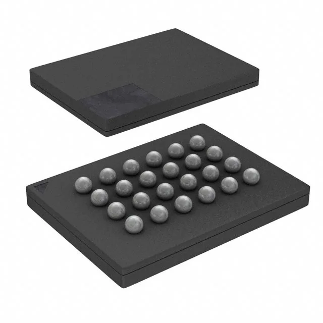
Cypress Semiconductor's S25FL116K0XBHIS30 is officially listed as Obsolete. For production builds that already have this part in the BOM, the only supply path is through independent distribution — surplus, new-old-stock, or broker-channel inventory. The date-code traceability and marking authenticity need close inspection when buying outside the authorized chain; the 24-TBGA package is a common target for re-marking due to its small footprint.
The S25FL116K0XBHIS30 is a 16 Mbit (2M × 8) NOR flash memory using a SPI Quad I/O interface running at up to 108 MHz clock frequency. NOR flash gives fast random-read access and execute-in-place (XIP) capability, which suits it for boot code, firmware storage, and parameter tables in embedded systems. The Quad I/O mode allows four-bit data transfers on a single clock, boosting throughput over standard SPI without adding pins — useful for code shadowing or OTA staging on resource-constrained MCUs.
24-TBGA footprint — layout considerations
BGA packages require via-in-pad or microvia routing for signal breakout, and a solder-mask-defined pad geometry. The 0.8 mm ball pitch is manageable with standard PCB fab processes, but the board house must support BGA assembly and X-ray inspection.
Write cycle time and endurance context
Page and word write cycles are rated at 3 ms typical. For a 256-byte page program, that translates to roughly 130 KB/s sustained write throughput in single-plane mode — adequate for configuration storage and firmware updates, but not for high-speed data logging. NOR flash endurance is typically 100k erase cycles per sector (though not explicitly stated in this listing); the 3 ms write time is consistent with that class. If the application does frequent parameter updates, consider wear-leveling in software or a separate serial EEPROM.