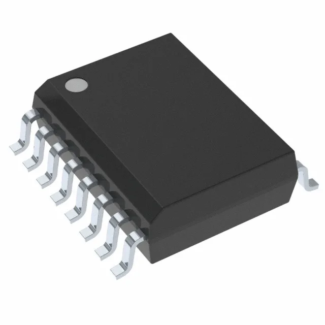
Infineon Technologies S25FL064P0XMFV000 — Memory (DRAM / SRAM / Flash / EEPROM)

S25FL064P0XMFV000 64 Mbit NOR Flash, 104 MHz Quad-SPI

MPNS25FL064P0XMFV000
Obsolete

Infineon/Cypress FL-P series, S25FL064P0XMFV000, 64 Mbit NOR Flash memory, SPI - Quad I/O, 104 MHz clock, 2.7V–3.6V supply, -40°C to 105°C, 16-SOIC package.

Sourced new & surplus through independent channelsAuthenticity-screened · ESD-safe packingListing updated Jul 2026

Specifications

S25FL064P0XMFV000 specifications
ParameterValue
SeriesFL-P
Memory typeNon-Volatile
MountingSurface Mount
Voltage2.7V ~ 3.6V
Frequency104 MHz
Memory interfaceSPI - Quad I/O
Operating temperature-40°C ~ 105°C (TA)
PackageTray
TechnologyFLASH - NOR
Memory size64Mbit
Memory formatFLASH
Case16-SOIC (0.295\", 7.50mm Width)
Memory organization8M x 8
Write cycle time - word, page5µs, 3ms

Product details

The Infineon (formerly Cypress) S25FL064P0XMFV000 is a 64 Mbit serial NOR Flash memory from the FL-P family, organized as 8M x 8 bits. The 104 MHz clock rate means a quad-read burst can deliver around 50 MB/s — enough for shadowing a small FPGA configuration or holding a boot image that the host MCU executes in place.

Obsolete — last-time-buy reality and sourcing posture

New production has ended, and the only available channel is the surplus and broker market. If you are qualifying this for a new BOM line, you need to identify a pin-compatible alternative now — the FL-P family has been superseded by newer NOR Flash families from Infineon and other vendors.

104 MHz Quad-SPI — what the clock rate means for the bus

The 104 MHz clock frequency is the maximum SPI clock the device supports. At this rate, a quad-read instruction (0xEB) reads four bits per clock, giving a raw data rate of 416 Mbps. For a host controller that supports Quad-SPI, this is fast enough to run code directly from the Flash (execute-in-place, or XiP) without a RAM shadow — provided the controller's memory-mapped Quad-SPI interface can keep up. The write cycle times are 5 µs for a page and 3 ms for a sector erase, which is typical for 65 nm NOR Flash. If your application does frequent small writes, budget for the sector-erase latency in the firmware state machine.

16-SOIC package — footprint and layout notes

The supplier device package is 16-SOIC, so the land pattern matches the JEDEC MO-119 variation for wide-body SOIC. No exposed thermal pad — the package dissipates through the leads, so keep the copper pour under the part connected to the ground plane for a modest thermal path.

Frequently asked questions

Where can I buy S25FL064P0XMFV000?

This part is obsolete and no longer in production. Submit a request for current availability and pricing — the quote will reflect the surplus market conditions at that time.

What is the replacement for S25FL064P0XMFV000?

There is no official successor listed for this specific order code. The FL-P series has been superseded by newer NOR Flash families. For a pin-compatible drop-in, look at the S25FL128P or S25FL256P variants in the same package — they share the same footprint and Quad-SPI interface, though firmware may need minor timing adjustments. Qualifying an alternate now is the prudent move given the obsolete status.

Is S25FL064P0XMFV000 compatible with the S25FL064Pxxx series?

Yes, the S25FL064P0XMFV000 is part of the FL-P series. Other density variants in the same package (e.g., S25FL032P, S25FL128P) share the same pinout and command set, making them hardware-compatible for a board spin. The main difference is memory density, which the host firmware must handle through the appropriate ID and sector-mapping routines.