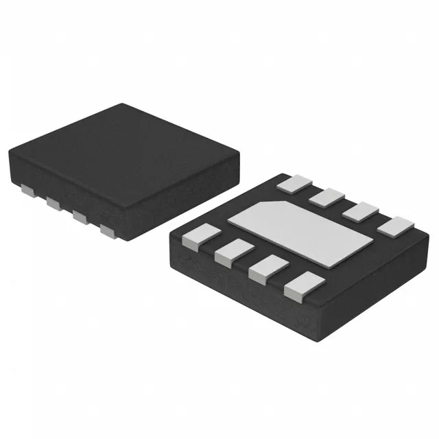
It communicates over a SPI bus with Quad I/O and QPI support, clocked at up to 108 MHz. That clock rate, combined with the quad-wide data path, gives a sustained read throughput that keeps a Cortex-M or RISC-V core fed during execute-in-place (XIP) boot without stalling for wait states. The memory is non-volatile and uses NOR Flash technology, which means byte- or page-addressable random access — not just block-oriented like NAND. That matters for firmware storage where you need to execute code directly or update a single configuration word without erasing a whole sector.
125°C operating temperature — industrial and under-hood ready
The 8-USON (4x4) package with exposed pad helps pull heat out of the die into the PCB copper plane. The pad is not just a thermal path — it also serves as a ground reference for the SPI signals, so a solid via stitch under the package improves both thermal and signal integrity.
Standard SPI uses one data line each way. Quad I/O uses four data lines for both read and write, quadrupling the throughput without raising the clock frequency. QPI (Quad Peripheral Interface) extends that to the command phase as well, so even the instruction opcode is sent over four pins. The practical effect: a 1 MB firmware image that takes ~80 ms to load over single SPI at 108 MHz reads in about 20 ms in Quad I/O mode. That difference can decide whether your system meets a power-on-to-main-loop timing requirement.
Infineon lists the S25FL064LABNFN043 as Active. The base product number S25FL064 covers a family of density and package variants, so if a future board spin needs a different footprint or temperature range, the migration stays within the same die family.
Sourcing and quoting
If you are qualifying this for a production BOM, the active lifecycle means you can commit the line without chasing a last-time buy.