Automotive-grade NOR Flash with 108 MHz Quad SPI
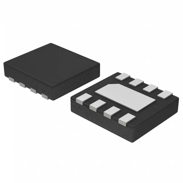
It uses a SPI interface with Quad I/O and QPI support, clocked at 108 MHz, and is organized as 8M x 8 bits. This part is intended for automotive electronic control units, ADAS modules, and other systems requiring reliable non-volatile storage in high-temperature environments. The compact 8-USON (4x4) package with exposed pad suits space-constrained board layouts where thermal dissipation through the pad is needed.
108 MHz clock and Quad SPI — what it means for read throughput
The 108 MHz clock on the SPI bus, combined with Quad I/O, gives a peak read throughput that can keep a high-speed MCU fed for code shadowing or data logging without stalling. At 108 MHz quad-read, each cycle transfers 4 bits, so the effective data rate is 432 Mbit/s. That is enough to fill a 64 Mbit device in under 150 ms — fast enough for over-the-air update staging or boot-from-external-Flash designs. The QPI mode reduces the command overhead by using the same four lines for address and data, which helps when the bus is shared.
There is no last-time-buy window or end-of-life notice to track. The base product number is S25FL064, so density variants in the same package family share the same footprint and interface.
Package and thermal pad — layout considerations
The device is supplied in an 8-UDFN exposed-pad package, also designated as 8-USON (4x4). Without that, the junction temperature can exceed the 105°C ambient rating under continuous read operation. The mounting is surface-mount, and the shipping medium is Tray.