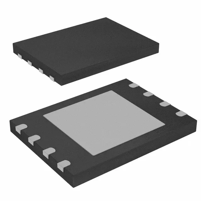
The S25FL032P0XNFA010 is classified as Obsolete by Infineon Technologies, meaning the manufacturer has ceased production with no scheduled last-time-buy window remaining. Availability is limited to independent surplus and broker channels. Each lot is traceable and physically authenticated — date-code consistency, marking integrity, and package condition verified before shipment. For BOM continuity, confirm the functional requirements against the 32 Mbit density, SPI Quad I/O interface, and 8-WSON footprint before committing to a surplus lot.
32 Mbit SPI NOR Flash with 104 MHz quad-I/O
Organized as 4M x 8 bits, this NOR flash delivers 104 MHz clock frequency over a SPI Quad I/O interface — the quad-lane read mode quadruples throughput over single-bit SPI, suiting code-shadowing and fast boot applications where the CPU executes directly from the flash. Write cycle timing is 5 µs for a word and 3 ms for a page, which sets the firmware update window — a full 32 Mbit erase and rewrite cycle must budget the sector erase time (typically 45 ms per sector) plus the page program time.
AEC-Q100 qualification and package
The FL-P series carries AEC-Q100 automotive qualification (Grade 3, -40°C to 85°C), meaning it has passed the stress tests and reliability screening required for production-vehicle electronics — temperature cycling, ESD, latch-up, and extended endurance validation per the AEC-Q100 test flow. Packaged in an 8-WDFN exposed pad (8-WSON, 6x8 mm), the thermal pad under the die provides a low-thermal-resistance path to the PCB copper plane — essential for dissipating self-heating during continuous read bursts at 104 MHz. The exposed pad footprint requires a thermal via array in the PCB layout to achieve the rated junction-to-ambient thermal resistance. Supplied in tray format; the base product number S25FL032 identifies the family for cross-referencing datasheets and application notes.