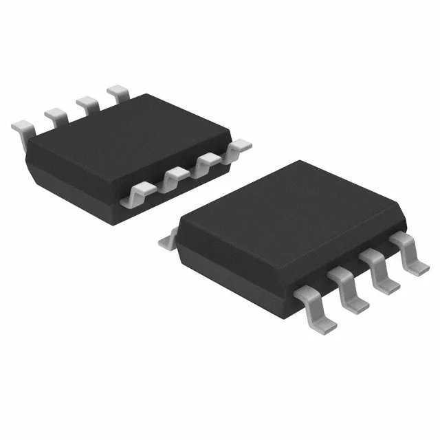
32 Mbit NOR Flash with Quad-SPI — what it delivers
The 104 MHz clock rate with Quad I/O yields a practical read throughput that supports execute-in-place (XIP) code execution or fast firmware staging for an external MCU or FPGA. The memory operates from a single 2.7V to 3.6V supply, covering the standard 3.3V rail with enough headroom for brownout conditions. Write-cycle timing is 5 µs for a word and 3 ms for a page, which is fast enough for OTA update staging and configuration parameter storage.
The FL-P series has been superseded by newer NOR Flash families with higher density and faster interfaces.
104 MHz Quad I/O — real-world throughput for the bus
The 104 MHz clock frequency with Quad I/O interface is the headline performance spec. At 104 MHz with four data lines, the sustained read throughput approaches 52 MB/s in fast-read quad mode. That is enough to feed a 32-bit MCU executing code directly from the flash (XIP) without a separate RAM copy for most control-loop and protocol-stack workloads. The Quad I/O mode uses the same four pins as standard SPI but reconfigures them as bidirectional data lines — no extra PCB traces needed. The 5 µs word-program time and 3 ms page-program time mean that writing a full 256-byte page takes about 3 ms. For OTA update scenarios where a 1 MB firmware image is written sector by sector, budget roughly 12 seconds for the erase and program cycle, assuming 64 KB sector erase at typical 1-second-per-sector rates.
Package and supply — fits standard 3.3V SPI Flash footprints
The supply range of 2.7V to 3.6V covers the 3.3V nominal rail with tolerance for transients down to 2.7V — useful for battery-backed or capacitor-held supplies during power loss.