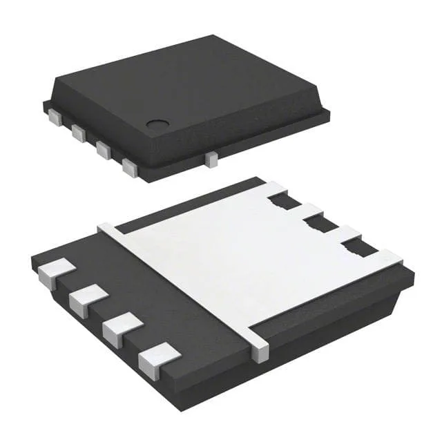
Infineon Technologies ISC0805NLSATMA1

Infineon ISC0805NLSATMA1 N-Channel MOSFET, 100V, 7.8mOhm

MPNISC0805NLSATMA1
End of Life

Infineon OptiMOS™ 5 ISC0805NLSATMA1, N-Channel MOSFET, 100V Vdss, 7.8mOhm Rds(on) @ 50A/10V, 33nC Qg, 13A/71A Id, PG-TDSON-8-46, -55 to 150°C.

$2.26Ref. price · indicative, final on quote
Packaging8-PowerTDFN
StockContact for availability
MOQ1 pcs
  • 100% new & originalTraceable channels only — no refurbs, no pulls, no remarked parts.
  • Date & lot codes on quoteStated per line before you commit; label photos on request.
  • MSL-compliant ESD packingMoisture-sealed bags with indicator cards; reels photo-verified.
  • PayPal buyer protectionPay by T/T, PayPal or Payoneer — card payments covered end to end.

Specifications

ISC0805NLSATMA1 Technical Specifications
ParameterValue
SeriesOptiMOS™ 5
FET typeN-Channel
Mounting typeSurface Mount
Drain to source voltage100 V
Drive voltage (Max rds on, min rds on)4.5V, 10V
Current - continuous drain (Id) @ 25°C13A (Ta), 71A (Tc)
Power dissipation2.5W (Ta), 74W (Tc)
Operating temperature-55°C ~ 150°C (TJ)
PackageTape & Reel (TR); Cut Tape (CT)
Vgs±20V
TechnologyMOSFET (Metal Oxide)
Case8-PowerTDFN
Vgs(th) (Max) @ id2.3V @ 40µA
Rds on (Max) @ id, vgs7.8mOhm @ 50A, 10V
Gate charge (Qg) (Max) @ vgs33 nC @ 10 V
Input capacitance (Ciss) (Max) @ vds2200 pF @ 50 V

Product details

100V N-channel in a compact TDSON — what it delivers

The Infineon ISC0805NLSATMA1 is an N-channel MOSFET from the OptiMOS™ 5 family, rated for 100 V drain-to-source and a maximum continuous drain current of 13 A at ambient or 71 A when the case is heatsunk. The on-resistance maxes out at 7.8 mOhm with a 10 V gate drive, which keeps conduction losses low in a switching or linear role. The gate charge is 33 nC at 10 V, a figure that tells you the gate-drive energy per cycle and helps size the driver for the switching frequency you plan to run. The part comes in an 8-lead PowerTDFN package (PG-TDSON-8-46), a surface-mount footprint that keeps the board area small while the exposed pad pulls heat into the PCB copper. The junction temperature range spans -55°C to 150°C, so it fits automotive under-hood, industrial motor drives, and outdoor telecom equipment where the ambient runs hot.

Rds(on) and gate charge — what they mean for the switching design

The 7.8 mOhm maximum at 50 A and 10 V is the number to use for worst-case conduction loss calculations in a buck converter, OR-ing diode replacement, or load switch. The drive voltage range is 4.5 V to 10 V, but the full Rds(on) spec is guaranteed at 10 V; if you run a 5 V gate drive, expect a higher on-resistance and factor that into the thermal budget. With 33 nC of gate charge at 10 V, the ISC0805NLSATMA1 is not a high-Qg part — it switches cleanly with a standard gate driver IC. The input capacitance is 2200 pF at 50 V drain bias, which gives a rough idea of the drive current needed to hit a target rise time. For a 100 kHz hard-switched converter, the gate-drive loss stays manageable.

Package and thermal reality

The PG-TDSON-8-46 package is a surface-mount PowerTDFN with an exposed drain pad. The dual current rating — 13 A at ambient (2.5 W max) and 71 A at case temperature (74 W max) — is the practical design split: the 71 A figure assumes you have a good thermal path to a heatsink or a multi-layer board with thermal vias. Without that, the ambient rating is the binding limit.

Lifecycle and sourcing

The ISC0805NLSATMA1 is listed as Active in production with ROHS3 compliance. There is no last-time-buy notice or NRND flag on this part, so it remains a safe choice for new designs and production BOMs. The OptiMOS™ 5 family is Infineon's mainstream 100 V trench technology, widely stocked across the distribution channel.

Frequently asked questions

Does ISC0805NLSATMA1 have a lead-free package?

Yes, the part is ROHS3 compliant, which means it meets the lead-free and RoHS exemption requirements.