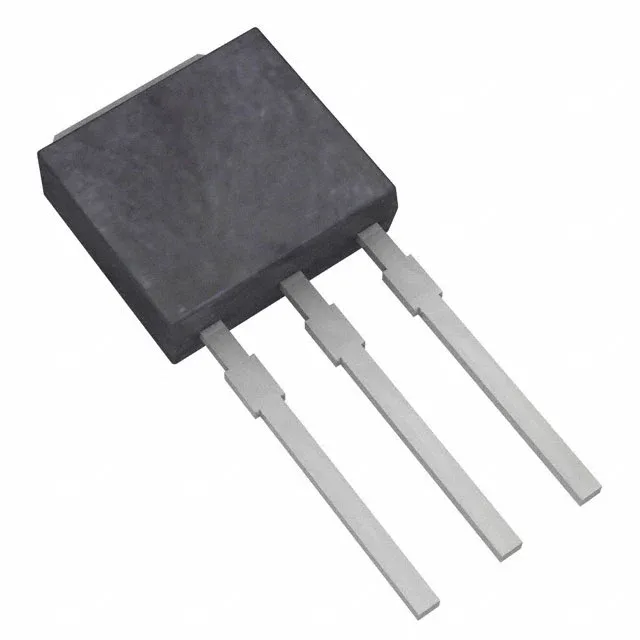
55 V, 17 A N-channel HEXFET in a TO-251AA IPAK
Switching and drive characteristics for BOM planning
Total gate charge is 15 nC at a 5 V gate-source voltage, low enough that a standard 5 V logic output can drive the gate directly in moderate-frequency switching applications, eliminating a dedicated gate-driver IC. Input capacitance (Ciss) is 480 pF typical at 25 V drain-source bias, which together with the gate charge sets the switching energy per cycle for the upstream driver. Maximum power dissipation is 45 W at 25 °C case temperature; derate above that per the datasheet's thermal impedance curve.
Through-hole IPAK package and temperature grade
The IPAK footprint is more compact than a standard TO-220 and suits high-vibration environments where a surface-mount package would risk solder-joint fatigue. The maximum gate-source voltage is ±16 V, allowing the part to tolerate 15 V gate-drive rails common in industrial power stages.
No stock-holding claim; quoted per BOM quantity.