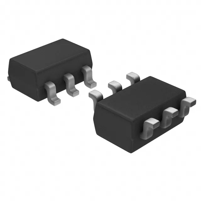
The 17.5 mOhm on-resistance at 4.5 Vgs keeps conduction losses low in a 3 A to 5 A load path — at 5 A the dissipation is under 0.5 W, which the SOT-23-6 can sink with a decent copper pour on the drain pad. The total gate charge of 11 nC at 4.5 V means the gate driver sees a light capacitive load; a 1 A driver switches the FET in under 15 ns, so the switching edge is fast enough for a 100 kHz to 200 kHz buck converter without excessive cross-conduction.
SOT-23-6 rework and board integration
The SOT-23-6 package has a 0.95 mm pitch and a small body — the drain tab is on the centre pins (pins 4, 5, 6), so the PCB layout should tie those together with a thermal-relief via to an inner-layer copper plane. The part is rated for a maximum power dissipation of 2 W at 25°C ambient, but that assumes a standard FR-4 board with minimal copper; real-world continuous dissipation is closer to 1 W for a 1 oz pour. Under a hot-air rework station, the small package heats quickly — use a 300°C nozzle at low airflow and lift the part when the solder on all six joints is molten, not before.